
TA7366 67 five lights single drive circuit

The TA 7366/7367 display driver circuit is designed to provide efficient LED driving capabilities for visual indicators in various electronic applications. The circuit's architecture, which incorporates a 9-pin configuration, allows for compact integration into devices where space is limited.
The operational amplifier within the circuit plays a crucial role by amplifying the input signal. This amplification is essential for ensuring that the signal reaches a level sufficient to drive the LEDs effectively. The subsequent five voltage comparator stages serve to monitor the amplified signal against a predetermined reference voltage. This functionality allows for precise control over the LED illumination based on the input signal's characteristics.
In the TA7366 variant, the display driver can manage up to five LEDs, with each LED corresponding to specific gain levels. The gain settings are tailored to provide a range of display outputs, from 0 to 16 dB, with specific intervals that enhance the visibility of the output signal. For instance, the intervals for the TA7366 are set at 3, 3.5, and 5 dB, while the TA7367 offers a more granular control with 2 dB intervals.
The power supply requirements for both circuits range from 4 to 12V, making them versatile for various power supply configurations. The quiescent current of 3mA indicates low power consumption during idle operation, which is beneficial for battery-powered applications. The output current capability of 8mA ensures that the LEDs can be driven effectively without risking damage to the components.
Overall, the TA 7366/7367 display driver circuits are well-suited for applications requiring reliable LED indication, such as audio level meters, signal strength indicators, and other visual feedback systems in consumer electronics. Their design offers a balance between performance and efficiency, making them a preferred choice among engineers and designers. Commonly used single display driver circuit TA 7366/7367 is manufactured by Toshiba Corporation 5 LED driver circuit, it adopted a 9-pin single in-line with plastic structure, within which the circuit configuration and application circuit of the circuit shown in Figure 4-48 o intron 6 op amp and a reference voltage circuit. 6 op amp as an input amplifier for amplifying the input signal to obtain sufficient drive level, and the remaining five groups consisting of five voltage comparator stage 05 and voltage comparator reference voltage ratio comparing, when the input when the signal level is greater than the reference voltage, the comparator output is low, driving the stage light emitting diode emits light.
For TA7366, its fifth light-emitting diodes k clever to zero level in turn is a 3 and b is supported, LD is a 6dB, Lm is a iicB, LDI is a 16 blood. For TA7367. LD5 is OdB, k 2 is a nosebleed, k is a 4dB, Lm is a 6dB, LD1 is a 8dB. Difference between the two drive circuits, one maximum display range: 0 to a one 16dB, one of O ~ a 8dB; the second is the level of each interval different: one interval 3,3.5, SdB, a only intervals are 2dB.
The remaining two electrical parameters, power supply voltage range V : 4 ~ 12V; quiescent current, : 3mA; output stream 8rnA; lighting sensitivity V : 230mV (fifth only lights) o
Related Circuits
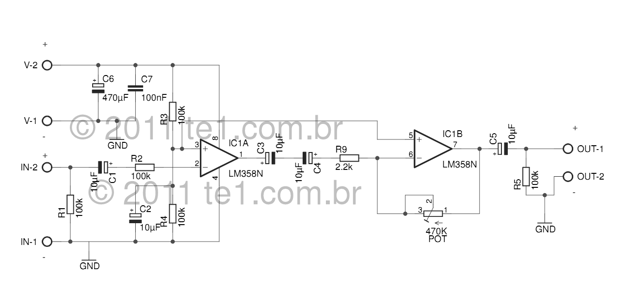
The LM358 series consists of two independent, high-gain, internally frequency-compensated operational amplifiers designed specifically to operate from a single power supply over a wide range of voltages. Operation from split power supplies is also possible, and the low power...
This is a fire alarm system utilizing the IC TD2002 suite to detect fire incidents. The alarm is crucial in residential complexes, allowing for early detection. It operates by detecting fog generated by fire, which reduces the light reaching...
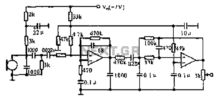
The CX9800 models of mobile phones and desktop PCs feature a high-performance voice processing circuit that compresses the amplitude and bandwidth of the microphone signal. This design enhances the sensitivity of the microphone and its adaptability to varying distances....
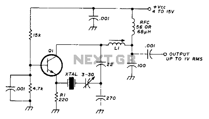
A circuit diagram illustrating the reliability of crystal startup, with power consumption significantly lower than the maximum allowed for the crystal. The transistor Q1 can be one of the following: 2N918, 2N3564, 2N5770, BF180, or BF200. The inductor L1...
This sound-controlled lighting circuit design is utilized to adjust the brightness of connected lights in synchronization with captured sound. The sound-controlled lighting circuit operates by detecting audio signals through a microphone or sound sensor. The circuit typically consists of several...
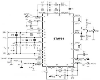
This is a stereo amplifier circuit diagram. The amplifier will produce stereo output channels with a power audio output that can reach up to 70W for each channel. The amplifier is built using the STA550 chip from STMicroelectronics. It...