
TDA1020 12W audio amplifier circuit design electronic project

The TDA1020 audio amplifier is engineered to deliver a maximum output power of 12 watts, making it suitable for driving speakers in automotive environments where space and efficiency are critical. The device operates on a supply voltage range typically between 12V to 14.4V, which aligns well with standard automotive electrical systems.
The amplifier features an internal short-circuit protection mechanism and thermal shutdown capabilities, ensuring robust operation under varying conditions. The 9-lead SIL package allows for easy integration into printed circuit boards (PCBs), facilitating compact designs that are essential in automotive applications.
Key specifications include a low total harmonic distortion (THD), which contributes to high-quality audio reproduction. The amplifier also supports a wide frequency response, typically ranging from 20 Hz to 20 kHz, ensuring that it can handle the full spectrum of audio signals effectively.
The input stage of the TDA1020 is designed to accept differential signals, which helps in minimizing noise and interference, a critical factor in automotive environments. Additionally, the output stage is capable of driving low-impedance loads, making it versatile for various speaker configurations.
In summary, the TDA1020 is a reliable and efficient audio amplifier that meets the demands of automotive audio systems while offering flexibility for broader audio applications. Its design principles prioritize performance, thermal management, and ease of integration, making it a valuable component for audio engineers and designers.The TDA1020 is a monolithic integrated 12 W audio amplifier in a 9-lead single in-line (SIL) plastic package designed as car audio amplifier but it can be used in many other audio applications. 🔗 External reference
Related Circuits
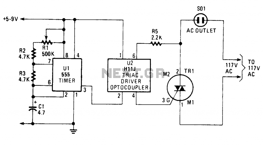
The blinking or flashing rate is determined by U1, a 555 timer integrated circuit. Its output, at pin 3, feeds U2, a H11J triac driver. That driver consists of an infrared LED that is coupled internally to a light-activated...
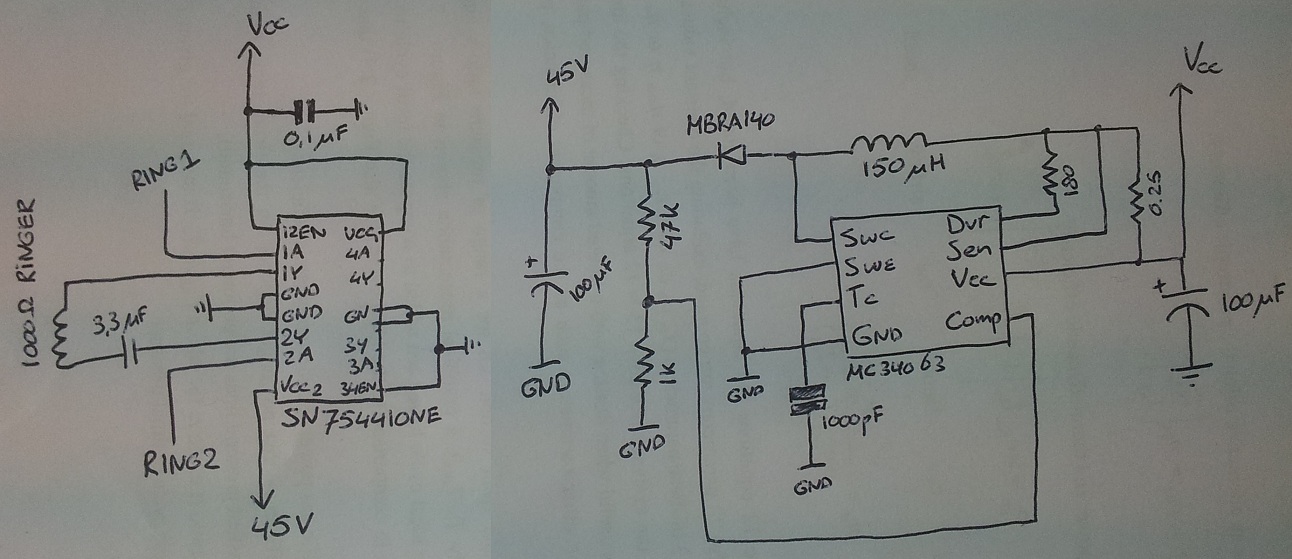
The process involves adapting an old phone for Bluetooth functionality, specifically testing the ringer circuit constructed using schematics from Sparkfun. When connecting a section of the schematic to a 3.5V source (Vcc), an output voltage of 45V is observed,...
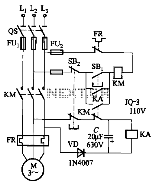
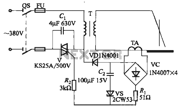
The circuit illustrated in Figure 3-73 is designed to utilize the power generated by instantaneous power failures, specifically the self-induced electromotive force (emf) produced by the motor, to implement an immediate shutdown protection mechanism. During a momentary power outage,...
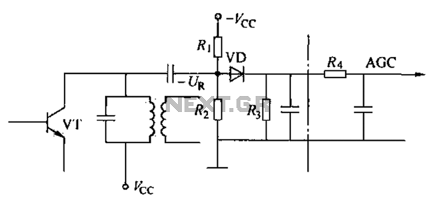
Commonly referred to as an automatic gain control (AGC) circuit, it is primarily utilized in receivers. This circuit maintains a constant output voltage amplitude despite variations in the input signal amplitude. It ensures that the receiver can effectively process...
The Triac V trigger voltage is less than 1V, and the trigger current is less than 30mA. The Triac is a semiconductor device commonly used for controlling AC power. It operates by allowing current to flow in both directions when...

The circuit depicted in Figure 3-200 (a) illustrates the operation of a reverse braking system. When reverse braking is initiated, the forward contacts of contactor KMi open, and the reverse brake contactor KM3 disconnects while the reverse contactor KM2...