
TDA6106Q having a feedback factor of the test circuit diagram 1 116

The TDA6106Q is a versatile integrated circuit designed for video applications, particularly in signal amplification and processing. The circuit architecture begins with the input stage, where the incoming video signal is filtered and conditioned using an input network composed of resistors R1 and R9, along with capacitors C1 and C2. This network ensures that the signal is appropriately scaled and shaped for optimal performance within the TDA6106Q's differential input stage.
The differential input stage is crucial for rejecting common-mode noise and enhancing the signal-to-noise ratio. The inverting input configuration allows for effective signal amplification, with the gain set by the feedback factor of 1/116, determined by the feedback network formed by R10 and Cpar. This feedback mechanism not only stabilizes the output but also plays a vital role in maintaining the black level of the video signal, ensuring consistent image quality.
The output stage, accessed through pin 8, is designed to drive subsequent stages or loads. The signal is further processed through a series of passive components, including resistors R2, R3 and capacitors C7, C8, C9, which can be configured to tailor the frequency response and output characteristics as needed for specific applications.
The inclusion of a bootstrap capacitor Cn between pins 8 and 9 enhances the dynamic range of the output, allowing the circuit to handle varying signal levels without distortion. This feature is particularly beneficial in video applications where signal integrity is paramount.
The cathode discharge protection mechanism integrated into pin 8 is a critical safety feature. It safeguards the circuit against voltage spikes that may occur from high-impedance sources, ensuring that the output can tolerate transient conditions without damage. The specifications indicate that it can handle significant current levels, making it robust for various operating environments.
Finally, the power supply requirements for the TDA6106Q necessitate the addition of decoupling capacitors at pin 6. These capacitors are essential for filtering out noise from the power supply, providing stable voltage levels to the IC, and ensuring reliable operation. Proper decoupling is crucial for maintaining the performance of the circuit, especially in high-frequency applications. Overall, the TDA6106Q test circuit exemplifies a well-designed approach to video signal amplification and processing, incorporating key features for stability, performance, and protection. As shown in FIG TDA6106Q test circuit with feedback factor is 1/116. After the input signal Vin from the input network R1, C1, C2, R9 enter TDA6106Q composed of 3 feet, 3 feet inside the differential input stage inverting input. The amplified signal from the 8-pin output, output through a network of R2, R3, C7, C8, C9 formed to probe. 3,9 feet between resistor R10 and capacitor Cpar feedback network, from the current automatic black level stabilizing role.
8,9 feet between the resistance and capacitance Cn bootstrap capacitor, the output from the expansion of the dynamic range of action. 8-pin output terminal having a cathode discharge protection, when the high-impedance source to generate a positive voltage spike discharges can withstand 100 C largest capacity 5A current; when the low-impedance source to generate a positive voltage spike discharges can withstand 100nC maximum 10A current capacity.
Power supply terminal (pin 6) must be added decoupling capacitors.
Related Circuits
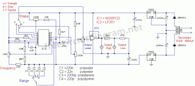
This is a simple function generator built around a single 8038 waveform generator IC. The circuit is capable of producing sine, square, or triangle waves within a frequency range of 20Hz to 200kHz. The function generator circuit utilizes the 8038...

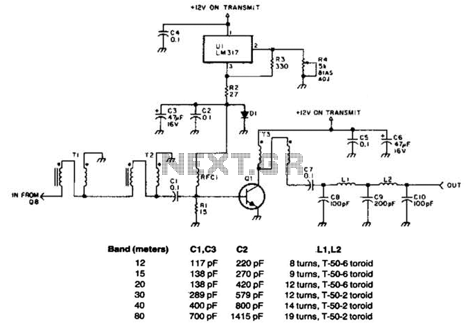
The LM317T is an adjustable three-terminal positive voltage regulator that can supply over 1.5 amps with an output voltage range of 1.25 to 37 volts. It features built-in current limiting and thermal shutdown, making it highly reliable and resistant...
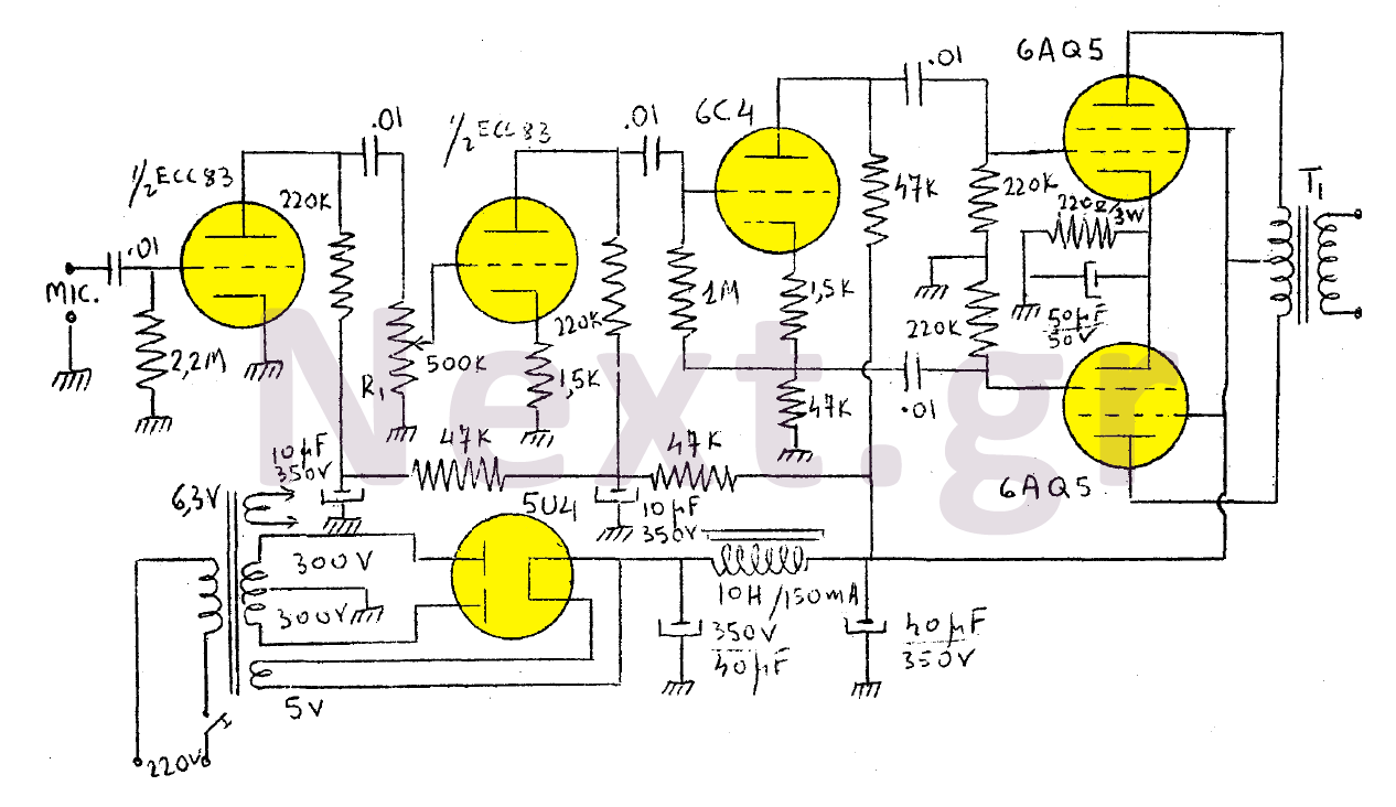
The output of this modulator consists of two 6AQ5 lamps arranged in a push-pull configuration with a maximum output of 15W. A 6C4 lamp is employed as a reversing lamp. The double-stage ESC83 serves as the pre-amplifier. The potentiometer...

Electronic FM Telephone Transmitter Schematic. The following schematic design illustrates a circuit diagram for an FM telephone transmitter built on a compact PC board layout. This small design allows it to be easily integrated within the housing of a...
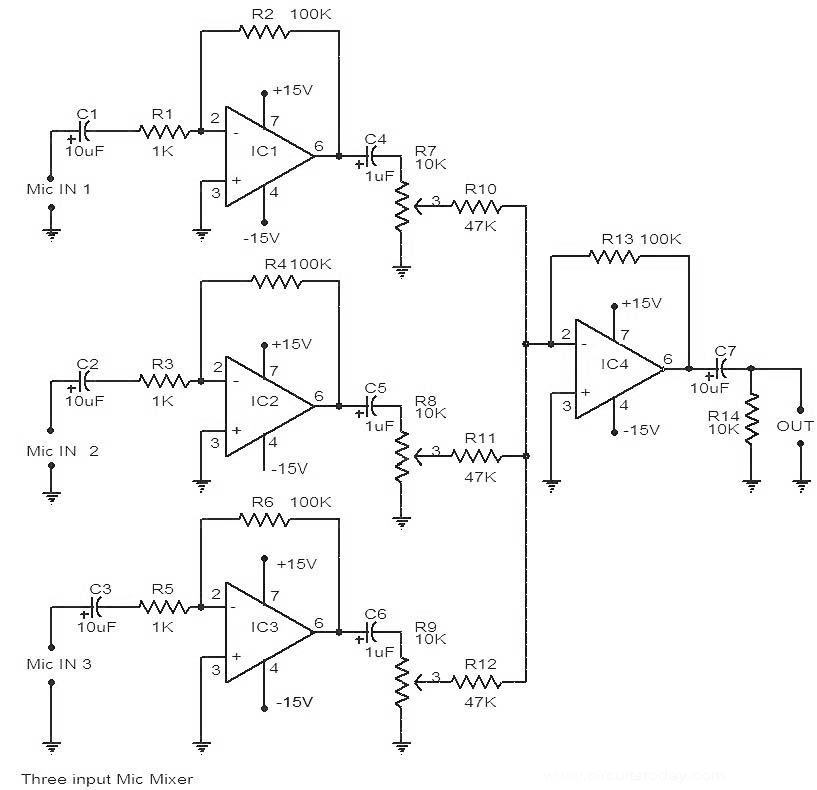
This is a circuit diagram of a 741 IC-based three-input microphone mixer circuit. A total of four 741 ICs are utilized, with IC1, IC2, and IC3 serving specific functions within the design. The circuit utilizes four operational amplifiers from the...
This linear amplifier provides a 10-W PEP output with a 1.25-W drive on the 10 m band. The transformers, T1, T2, and T3, consist of 10 turns of bifilar windings on an FT-50-43 toroidal core and are designed for...