
Test circuit diagram with feedback factor of 1 83 of TDA6120Q

The TDA6120Q is a versatile integrated circuit designed for use in various audio and video applications. It features a differential input stage that effectively amplifies the input signal while maintaining low noise levels. The configuration of resistors and capacitors in the circuit plays a crucial role in shaping the signal and ensuring stability.
The input stage, consisting of Ra, C10, and C11, serves to filter and condition the incoming signal before it reaches the differential inputs. This is critical for achieving high fidelity in the output. The differential inputs at pins 2 and 3 allow for common-mode noise rejection, enhancing the overall signal integrity.
The amplified output from pin 12 is further processed through a network of resistors and capacitors, which serve to adjust the frequency response and gain of the circuit. The feedback resistor (Rf) connected to pin 13 is integral to maintaining stability and controlling the gain of the amplifier, allowing for dynamic range expansion in the output signal.
The pre-emphasis network, formed by Ri, Rin, and C1, is essential for compensating for signal losses at higher frequencies, ensuring that the output maintains clarity and detail. This network is particularly important in applications where signal degradation may occur due to transmission over long distances.
The inclusion of Rflash at the output provides critical protection against voltage spikes, which can occur during sudden changes in load or external disturbances. This resistor limits the current and protects the circuit from potential damage, thereby enhancing the reliability of the system.
For proper operation, it is essential to include decoupling capacitors at Vcc and VDD. The use of both ceramic and electrolytic capacitors in parallel ensures that the circuit is adequately decoupled across a wide frequency range, minimizing the risk of oscillations and ensuring stable operation under varying load conditions. This design consideration is vital for maintaining the performance of the TDA6120Q in real-world applications.Feedback has shown TDA6120Q factor 1/83 test circuit shown in Figure. Input signal Vi composed by Ra, C10, C11 input into the network TDA6120Q 2 feet, 2 feet and 4 feet are ins ide the differential input stage inverting input terminal and non-inverting input, the amplified signal from 12 feet out, after by the Rflash, R2, R3, C7, C8, C9 network of output. Resistance between 13,5 feet Rf is the feedback network, the output from the expansion of the dynamic range of action.
Resistance between 1,3 feet Ri, Rin and capacitor C1 constitute a pre-emphasis network. The output end of the resistor Rflash cathode discharge protection, when a high voltage discharge, serves to limit the current and voltage limiting effect. Vcc (6 feet), VDD (10 feet) must be added decoupling capacitors, high-frequency decoupling capacitance characteristics of a good ceramic capacitors and electrolytic capacitors connected in parallel.
Related Circuits
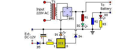
Mobile phone chargers available in the market are quite expensive. The circuit presented here serves as a low-cost alternative to charge mobile telephones or battery packs with a rating of 7.2 volts. The proposed circuit design utilizes a straightforward approach to...
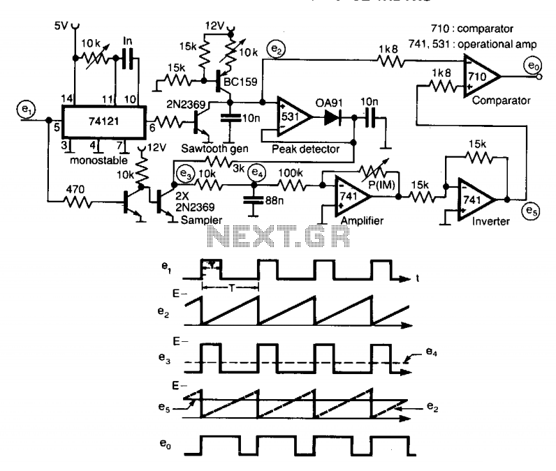
A circuit designed to multiply the width of incoming pulses by a factor that can be greater or less than unity is straightforward to construct. It features a single adjustable potentiometer for selecting the multiplying factor. This factor is...
A digital amplifier is a new device that IC manufacturers are eager to capitalize on, leading to the launch of unique digital amplifier products. Below are brief descriptions of some representative devices. The TA2022, produced by Tripath, is an...

The chart illustrates a clock designed for a competition, utilizing a 555 timer circuit. This circuit is characterized by its novel design, reliable performance, ease of assembly, and engaging functionality. The 555 timer is available in two types: bipolar...

The basic two-transistor flasher has become widely utilized in various applications due to its simplicity and versatility. It has been employed in circuits such as a micropower low battery indicator, a lightning detector, an off-line switching power supply, a...

The difference between these two ICs. A microcontroller is a specialized type of microprocessor designed to be self-sufficient and cost-effective, while a microprocessor is typically intended for general-purpose use, such as in personal computers (PCs). The microcontroller integrates several...