
The logic circuit diagram composed of photocoupler

The AND gate logic circuit, as represented in Figure 1, is a fundamental building block in digital electronics. The output P of the circuit is high (1) only when both inputs A and B are high (1). This behavior is crucial for applications where a specific condition must be met before an output is triggered. The use of photodiodes in Figure B enhances the versatility of the circuit, allowing it to respond to light signals. When both photodiodes are illuminated, they conduct, enabling the output to reach a high state. This configuration can be adapted to create various logic gates, such as OR, NAND, and NOR gates, which are essential for constructing complex digital systems.
Figure 2 showcases an AC coupling amplifier circuit, designed to amplify alternating current signals while blocking direct current components. This circuit typically consists of an operational amplifier (op-amp), resistors, and capacitors. The coupling capacitors allow AC signals to pass while preventing DC bias from affecting the subsequent stages of the circuit. The design is particularly useful in applications where it is necessary to isolate the AC signal from any DC offset, such as in audio processing or light signal detection. The amplifier's gain can be adjusted by selecting appropriate resistor values, providing flexibility in signal amplification according to the specific requirements of the application.Figure 1 is AND gate logic circuit. Its logic expression is P=A, Figure B has 2 photodiodes in series. When input logic level A=1, B=1, output P=1. In a similar way, itcan form Or gate, NAND gate, NOR gate and some other logic circuits. As shown in figure 2, it is a typical AC coupling amplifier circuit, which is suitable for selecting lightin.. 🔗 External reference
Related Circuits
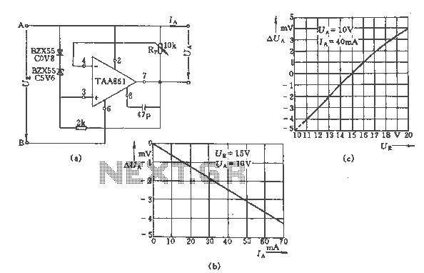
The regulator circuit adjusts the output voltage based on the potentiometer Rp and exhibits linear regulation characteristics. The output voltage Ua varies with the load current Ia, ranging from 0 to 70 mA, as illustrated in Figure (C) for...
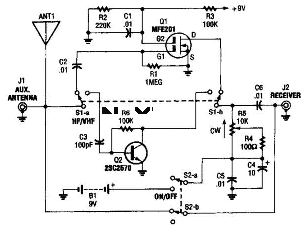
The AA-7 active antenna consists of two active components: Q1 (an MFE201 N-channel dual-gate FET) and Q2 (a 2SC2570 VHF silicon transistor), which form the foundation for two independent, switchable RF preamplifiers. The AA-7 active antenna is designed to enhance...
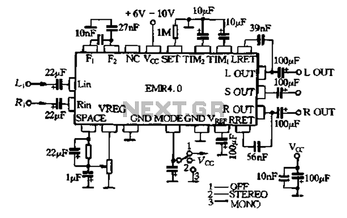
The EMR 4.0 operates with a single power supply ranging from 6V to 10V, with an optimal supply voltage of 9V. It requires effective power filtering to minimize noise, particularly when there is no signal input. The quiescent current...
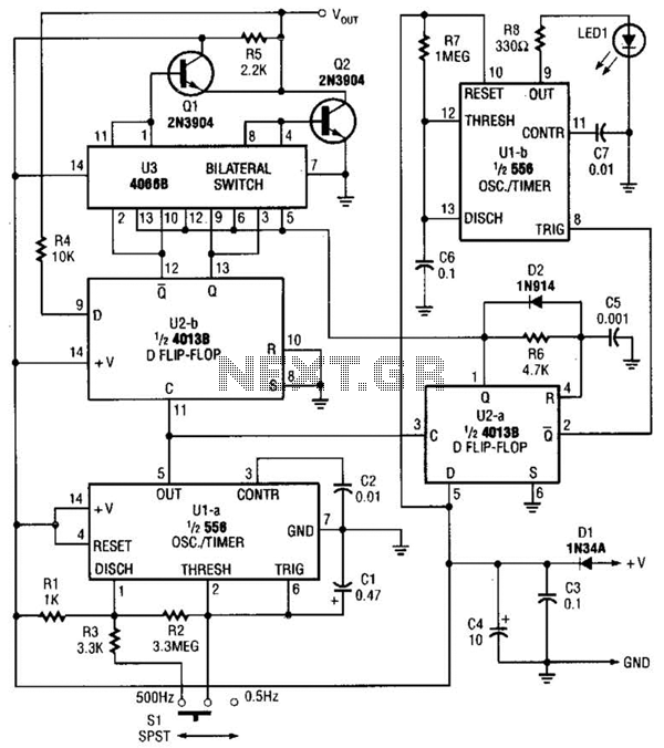
The logic pulser generates pulses at 500 Hz or 0.5 Hz. When the pulser's tip connects to an input that is already being driven high or low, the pulser senses the logic state and automatically pulses the input briefly...
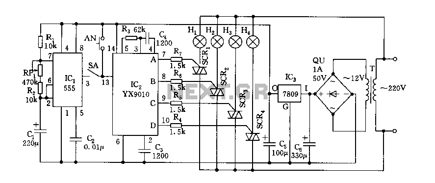
Fantasy lights offer wonderful changes suitable for storage, dance halls, or family holiday decorations. The control circuit is depicted here, which includes a multivibrator control circuit, a thyristor trigger circuit, and a step-down power supply circuit. The AC step-down...
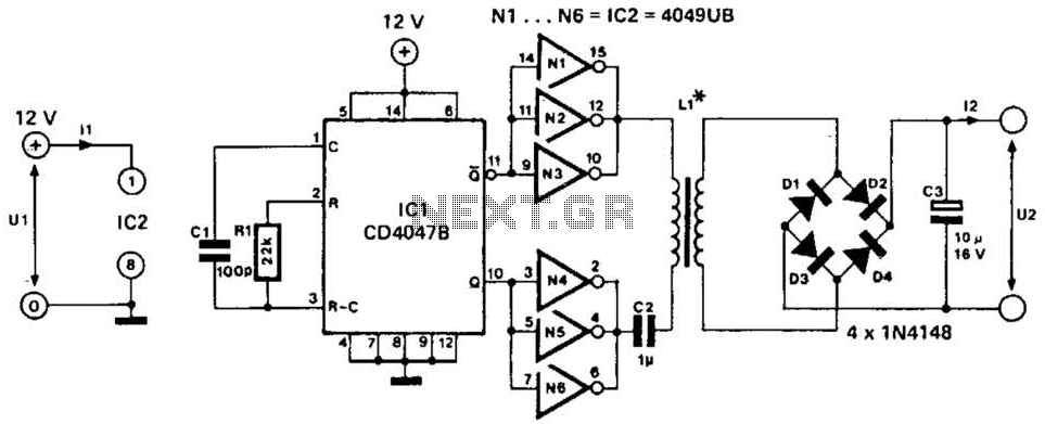
This low-power converter supplies approximately 100 mW of DC power to a load and is useful for isolating or deriving DC voltages. It operates at a frequency of around 200 kHz. The inductor is wound on a 22-mm diameter,...