
Three Phase protective circuit of the current detection line

The schematic involves a configuration of transistors designated as VTi, VT2, and VT3, which are integral to forming a gate structure. These transistors are typically arranged in a complementary manner, allowing for efficient switching and signal processing.
In this arrangement, VTi could represent a p-channel MOSFET, while VT2 and VT3 are likely n-channel MOSFETs. This complementary configuration enables the gate to achieve low power consumption and high-speed operation. The gate's functionality is crucial in digital circuits, where it can be used for logic operations or signal amplification.
The design may also include additional components such as resistors and capacitors for biasing and stability purposes. Proper biasing ensures that the transistors operate within their optimal regions, thus enhancing performance and reliability. The arrangement of these components should be carefully considered to minimize noise and improve signal integrity.
Overall, the described transistors and their configuration play a vital role in the functionality of the gate, influencing the overall performance of the electronic circuit in which they are implemented.Drawing, transistors constituting the gate VTi, VT2, VT3 and the like.
Related Circuits
The gain of the single-stage virtual earth amplifier IC1 is determined by the drain-source resistance of the field-effect transistor (FET). Resistors R1, R2, and R3 linearize the FET's voltage-current characteristic. A control voltage is derived from the output signal...
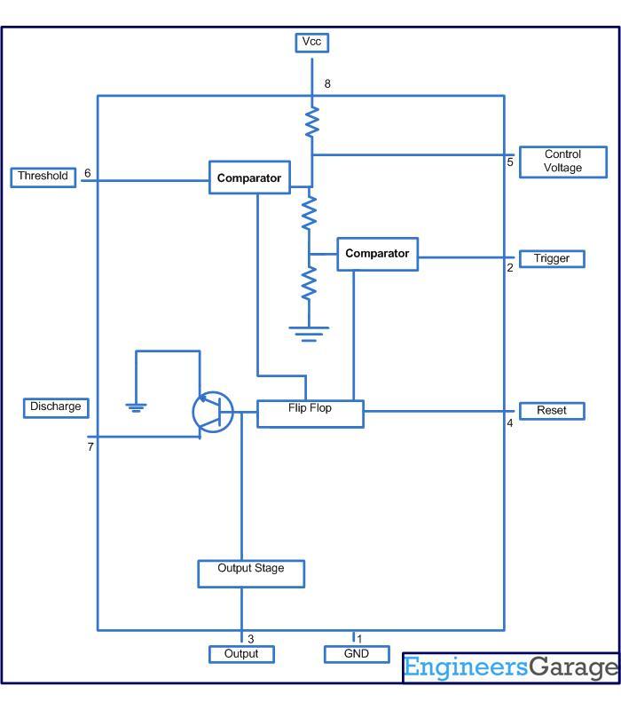
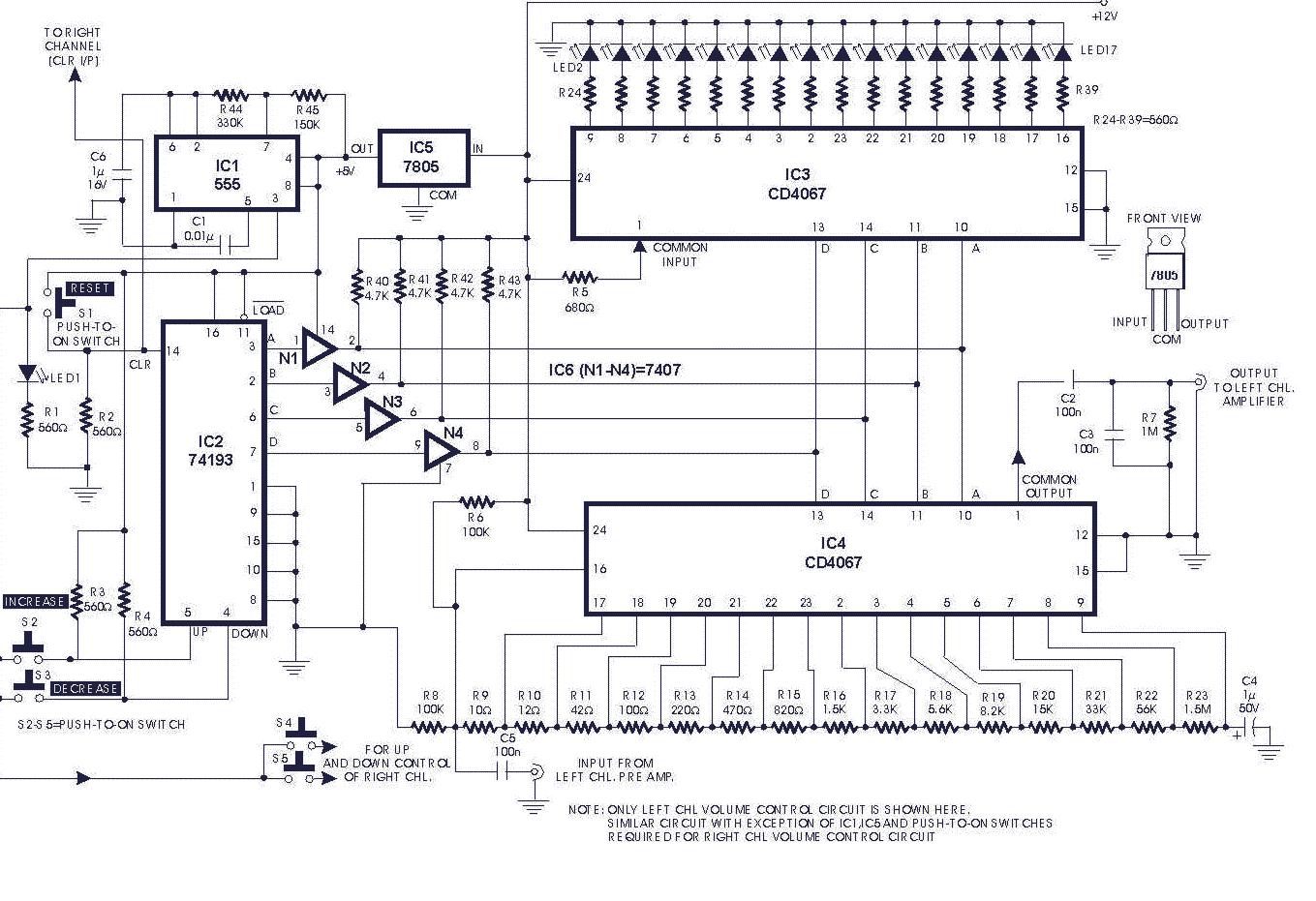
This circuit-based project demonstrates the operation of a 555 timer in astable mode to generate pulses with a time period of 0.5 seconds. These pulses can be utilized in various applications, such as blinking an LED or creating decorative...
The circuit is a battery charging system powered by Q2, Q6, R8, and D10, which provides constant current to charge the battery. When an external power supply is present, the charging current flows through R8 and D10 to charge...
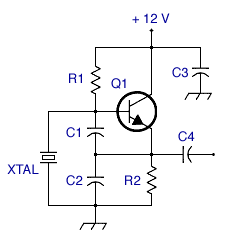
The circuit presented is a standard Colpitts oscillator, commonly utilized in many amateur radio homebrew transmitters. This specific circuit is designed to operate effectively within a frequency range of 1500 kHz to 8000 kHz. To accommodate lower frequencies, it...
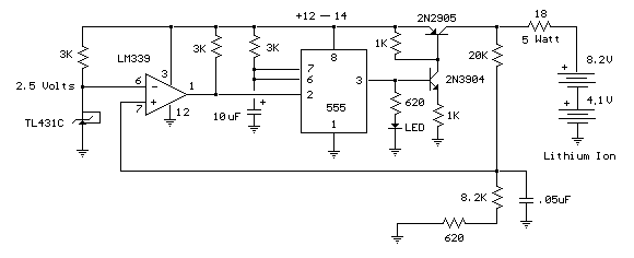
This circuit was built to charge two series lithium cells (3.6 volts each, 1 Amp Hour capacity) installed in a portable transistor radio. The circuit is designed to efficiently charge two lithium-ion cells connected in series. Each cell has a...
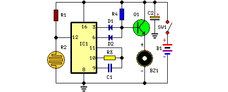
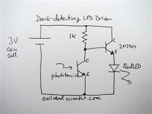
This circuit is housed in a compact enclosure and is positioned within the refrigerator, either near the lamp or at the door opening. When the refrigerator door is closed, the interior remains dark, causing the photoresistor R2 to exhibit...