
Thrifty 2Hz Clock

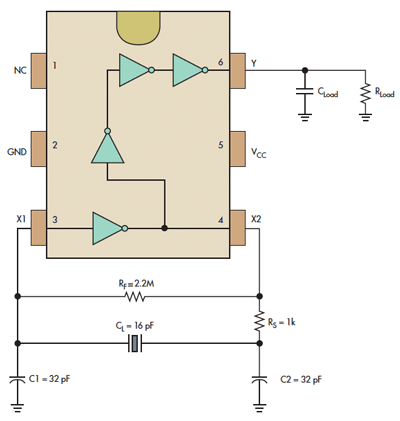
This oscillator circuit is designed to operate efficiently within low-power environments, making it ideal for portable and battery-operated devices. The use of a CMOS configuration ensures minimal power loss, which is advantageous in extending battery life. The LM334Z current source is a critical component, providing a stable and adjustable current supply, which is essential for maintaining the oscillator's performance without drawing excessive power.
The oscillator circuit employs a watch crystal, known for its precision and cost-effectiveness, to establish the frequency of oscillation. The surrounding passive components, including capacitors and resistors, are selected to optimize the performance of the oscillator, ensuring that it generates a stable frequency output. The 4060 frequency divider IC is utilized to further process the oscillation signal, effectively dividing the frequency down to the desired 2 Hz output, which can be used for timing applications or as a clock signal for other circuits.
The amplification and inversion stage using transistor T1 is necessary to ensure that the output signal from the oscillator meets the required voltage levels for subsequent circuitry. IC3a serves as a final stage in shaping the output waveform, providing a clean square wave with sharp transitions, which is crucial for digital applications where signal integrity is paramount. This careful design consideration allows the oscillator circuit to function reliably in various electronic applications while maintaining low power consumption.CMOS circuits are known for their low current consumption. This is particularly important for battery-powered circuits. Unfortunately, oscillators often require quite a bit of current. We therefore propose this oscillator circuit that has a very low current consumption (about 3 µA). The circuit is powered from a type LM334Z current source. The cu rrent has been set with R4 to about 3 µA. This is sufficient to power IC1 and the oscillator circuit around X1. The oscillator generates, with the aid of a cheap watch crystal and a few surrounding parts, a signal that is subsequently applied to the divider in the 4060 and results in a frequency of 2 Hz at pin 3 (output Q13). The level of the output pulses is a lot lower than the nominal 5-V power supply voltage (IC1 is after all powered from a current source with very low current).
That is why the signal on pin 3 of IC1 is amplified and inverted by T1. IC3a finally turns it into a proper square wave with acceptably steep edges. 🔗 External reference
Related Circuits
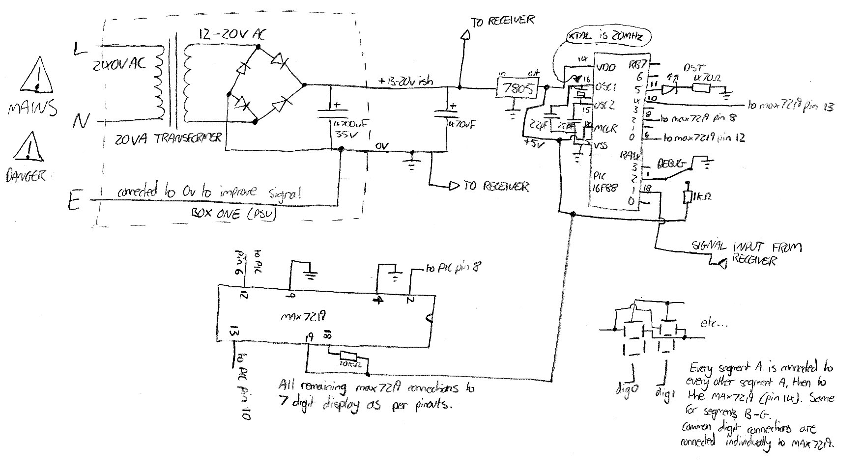
Detailing the design and build of a 60 kHz time code receiver and clock, from PIC programmer to LED clock display. The project involves the development of a 60 kHz time code receiver and clock system utilizing a microcontroller from...
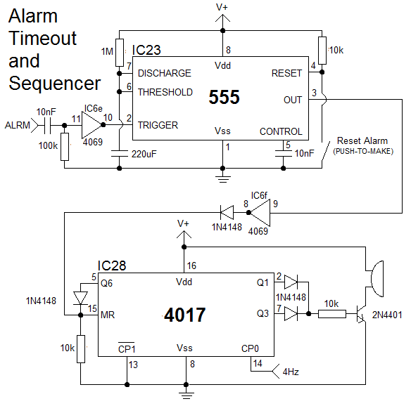
The clock is constructed using 25 CD4000 integrated circuits (ICs), three 555/556 ICs, and several discrete components. It features an alarm and a method for setting the time that is typically only seen in microcontroller designs. The complexity of...
TI's Dafydd Roche concludes his 4-part series on soundbar design with a thorough explanation of clock design for the digital section of the circuit. The clock design in digital circuits, particularly in soundbar applications, plays a crucial role in ensuring...
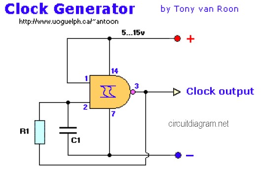
The following diagram is the clock generator circuit diagram built using NAND gate logic integrated circuits (ICs). The circuit can utilize either the IC 7400, which is a TTL type, or the IC 4011, which is a CMOS type....
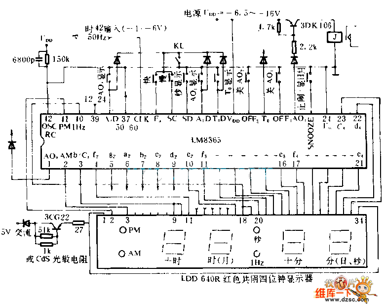
This electronic clock comprises the LM8365 and the LDD640R displays. The LM8365 can show the hour/minute and month/day. Users can set two alarm outputs, AD1 and AD2, by pressing either the 12h or 24h button. The operating voltage range...
This is a chronological account of a project to design and build a digital clock based on the Arduino open-source architecture, utilizing the ATMEGA8 microcontroller. The ATMEGA8 is an 8-bit, 16MHz microcontroller with integrated digital and analog inputs and...