
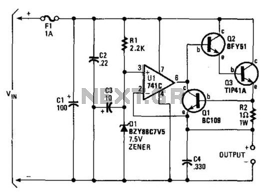
Transformerless 5 Volt Power Supply

The circuit design described employs a clever use of components to achieve a low-cost, low-part-count solution for powering small appliances from a mains supply. The inclusion of a JVR varistor for surge protection is critical, as it helps prevent damage from voltage spikes that can occur in mains electricity. The voltage divider formed by resistors R1 and R2 is essential for monitoring the rectified voltage and controlling the switching action of transistor T1. The feedback mechanism involving P1 allows for fine-tuning of the output current, ensuring that the circuit can adapt to varying load conditions while minimizing excess heat generation.
The soft start circuit, comprising T2, R3, and C2, is particularly important in applications where inrush current can cause damage to components or lead to instability in the power supply. By controlling the charging rate of C1, the circuit mitigates the risk of high initial currents, contributing to overall reliability.
The choice of zener diode D5 not only serves the purpose of voltage regulation but also acts as a protective element for C1, allowing for the use of lower voltage-rated capacitors, which can reduce overall costs. The design's consideration for current flow through R5 and D5 when the load is disconnected ensures that T3 remains protected from potentially damaging voltage levels, which enhances the circuit's robustness.
Overall, this circuit exemplifies an innovative approach to powering low-consumption devices from mains voltage, balancing efficiency, simplicity, and safety considerations. However, it is essential to emphasize the importance of adhering to safety standards when working with mains-powered circuits to prevent accidents and ensure safe operation.An increasing number of appliances draw a very small current from the power supply. If you need to design a mains powered device, you could generally choose between a linear and a switch-mode power supply. However, what if the appliance`s total power consumption is very small Transformer-based power supplies are bulky, while the switchers are gen
erally made to provide greater current output, with a significant increase in complexity, problems involving PCB layout and, inherently, reduced reliability. Is it possible to create a simple, minimum part-count mains (230 VAC primary) power supply, without transformers or coils, capable of delivering about 100 mA at, say, 5 V A general approach could be to employ a highly inefficient stabilizer that would rectify AC and, utilizing a zener diode to provide a 5.
1 V output, dissipate all the excess from 5. 1 V to (230G—v2) volts in a resistor. Even if the load would require only about 10 mA, the loss would be approximately 3 watts, so a significant heat dissipation would occur even for such a small power consumption. At 100 mA, the useless dissipation would go over 30 W, making this scheme completely unacceptable. Power conversion efficiency is not a major consideration here; instead, the basic problem is how to reduce heavy dissipation and protect the components from burning out.
The circuit shown here is one of the simplest ways to achieve the above goals in practice. A JVR varistor is used for overvoltage/surge protection. Voltage divider R1-R2 follows the rectified 230 V and, when it is high enough, T1 turns on and T3 cannot conduct. When the rectified voltage drops, T1 turns off and T3 starts to conduct current into the reservoir capacitor C1.
The interception point (the moment when T1 turns off) is set by P1 (usually set to about 3k3), which controls the total output current capacity of the power supply: reducing P1 makes T1 react later, stopping T3 later, so more current is supplied, but with increased heat dissipation. Components T2, R3 and C2 form a typical soft start` circuit to reduce current spikes this is necessary in order to limit C1`s charging current when the power supply is initially turned on.
At a given setting of P1, the output current through R5 is constant. Thus, load R4 takes as much current as it requires, while the rest goes through a zener diode, D5. Knowing the maximum current drawn by the load allows adjusting P1 to such a value as to provide a total current through R5 just 5 to 6 mA over the maximum required by the load. In this way, unnecessary dissipation is much reduced, with zener stabilization function preserved. Zener diode D5 also protects C1 from over voltages, thus enabling te use of low-cost 16 V electrolytics.
The current flow through R5 and D5, even when the load is disconnected, prevents T3`s gate-source voltage from rising too much and causing damage to device. In addition, T1 need not be a high-voltage transistor, but its current gain should exceed 120 (e. g. BC546B, or even BC547C can be used). The circuit is not galvanically isolated from the mains. Touching any part of the circuit (or any circuitry it supplies power to) while in operation, is dangerous and can result in an electric shock!
This circuit should not be built or used by individuals without proper knowledge of mains voltage procedures. 🔗 External reference
Related Circuits
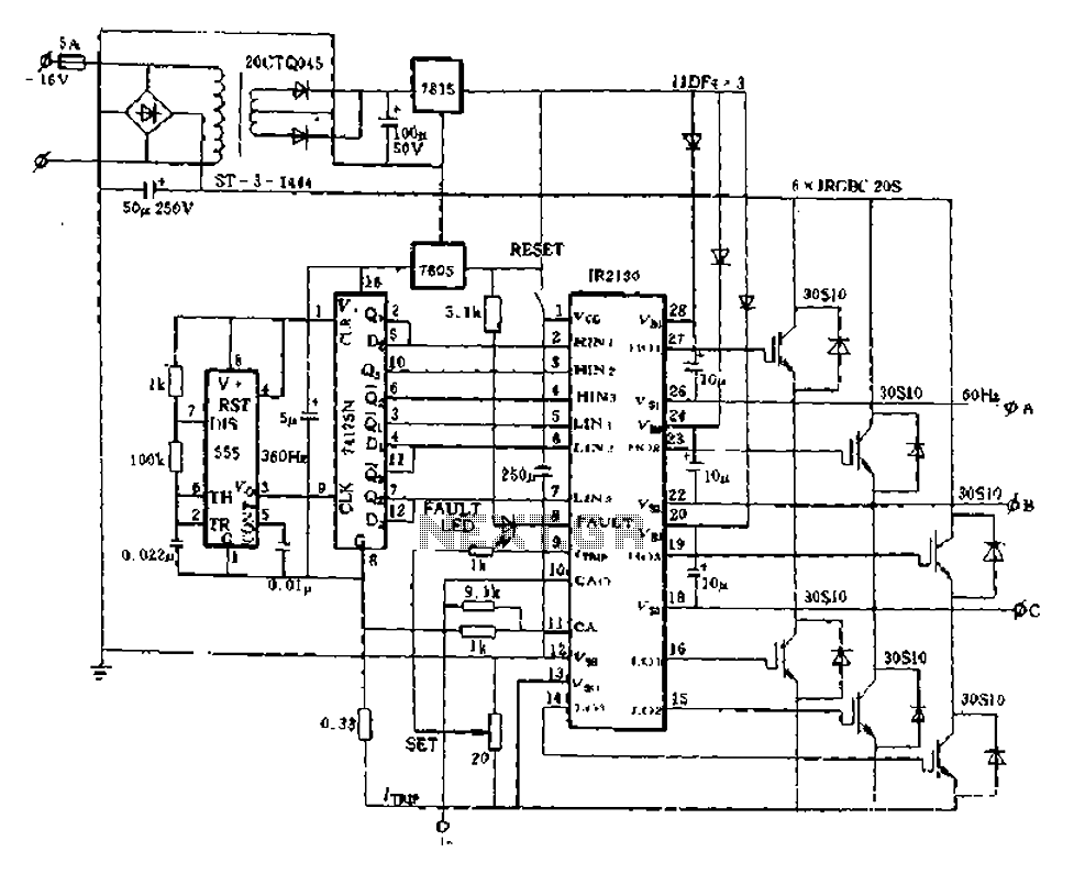
The application of the aforementioned advantages allows the IR2130 to be effectively utilized for DC cut crossing speed, DC servo systems, three-phase power inverters, and switching power supplies. Additionally, it is applicable in inverter power supplies, uninterruptible power supplies...
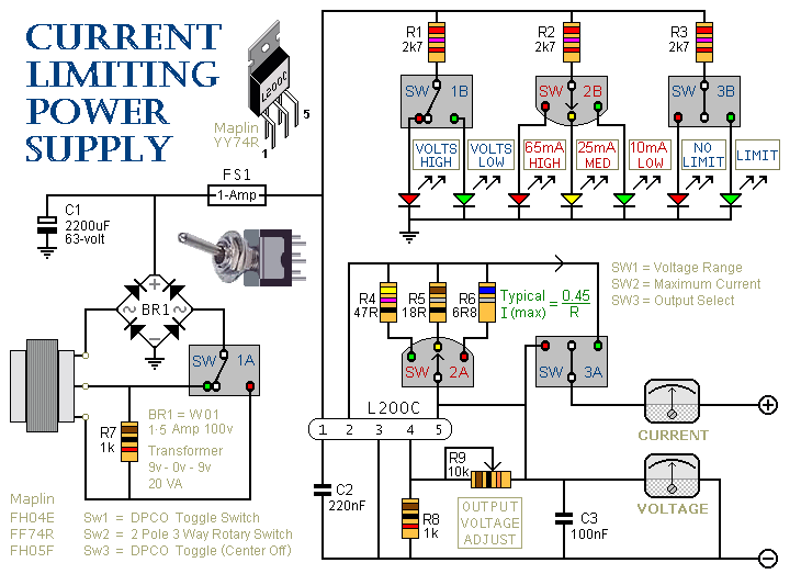
This is a 1-amp variable-voltage power supply unit (PSU) that adjusts the output voltage from approximately 3V to 24V. It features a current limiting option, which is particularly useful for initial power-ups or soak-testing equipment. SW3 acts as the...

This circuit provides emergency lighting during a power outage. The phototransistor should be positioned to maximize the coupling of both neon light and ambient light into the pellet, without allowing self-illumination from the 6-V lamp. Many circuits of this...
Expanding schematic circuit for the secondary circuit of high-voltage lines. The schematic circuit for the secondary circuit of high-voltage lines is designed to enhance the distribution and management of electrical power in high-voltage systems. This circuit typically includes components...
A regulator enables the powering of a 7.5-V cassette recorder or other devices from a 12-V DC automotive system. The circuit can provide approximately 600 mA of current. Q3 requires a heatsink due to its potential to dissipate up...
A complementary transistor pair (Q2 and Q3) is configured as a high-efficiency oscillator that directly drives the loudspeaker. Q1 is responsible for fully charging capacitor C2 when power is applied to the circuit. When switch P1 is pressed, C2...