
transistor amplifier self bias

The fixed-bias circuit for this transistor amplifier is a straightforward yet effective design, suitable for small-signal amplification applications. The choice of components is crucial for achieving optimal performance. The R1 resistor, typically set at 200 KΩ, is selected to establish a suitable base current that allows for the desired collector current based on the transistor's hFE. The load resistor R2, at 1 KΩ, ensures that the collector current remains within safe limits, preventing damage to the transistor during operation.
The coupling capacitors C1 and C2 play a vital role in the circuit by blocking any DC component from the input and output signals, allowing only the AC signals to pass through. This feature is essential for maintaining the integrity of the audio signal being amplified. The use of electrolytic capacitors rated for at least 10 µF and 6-10 VDC ensures that the capacitors can handle the voltage levels present in the circuit without failure.
In terms of performance, the amplifier is capable of handling low-level audio signals, making it ideal for use with microphones and other audio sources that produce similar signal levels. The gain of the amplifier, calculated at 80, indicates a significant increase in signal strength, facilitating better audio output when connected to devices such as crystal detector radios.
The design also incorporates protective features through negative feedback, which stabilizes the amplifier's performance under varying load conditions. As the collector current increases, the feedback mechanism reduces the base current, effectively preventing thermal runaway, which can lead to transistor failure.
Overall, this simple fixed-bias transistor amplifier circuit demonstrates the fundamental principles of transistor operation and biasing while providing a reliable solution for low-level audio amplification. The careful selection of components and design considerations ensures that the amplifier operates efficiently and safely within its specified parameters.The simplest way to bias a transistor amplifier is by the fixed-bias circuit. The supply voltage is connected to the transistor`s base terminal trough the R1 current limiting resistor. The value of the bias resistor is usually selected based on the transistor`s gain from its data sheet and the selected operating collector current.
Resistor R2 is t he load resistor for transistor Q1. The function of this R2 load resistor is to limit the collector current to safe values. The C1 and C2 coupling capacitors are used to separate the AC signals from the transistor`s DC bias current. Through these two capacitors, C1 and C2 connect the input and output AC [Alternating Current] signals.
In our simple, small signal, common emitter, transistor amplifier circuit the input signal is a 1 kHz 10 mV AC voltage. Usually microphones or turntable cartridges have similarly small signal levels. Thus our simple amplifier can be used to amplify similar low-level signals. Attaching the same amplifier to the output of a crystal detector radio would result in noticeable improvement in the output audio volume.
This amplifier outputs a 0. 8-Volt signal as shown by the red trace on the oscilloscope display - Figure 2. Notice that the output signal is not completely symmetrical, but the minor asymmetry does not affect the circuit operation. The scale for the blue trace is 10 mV per division and for the red trace it is 1 V per division. Since the gain of an amplifier is the ratio of the output to the input signal this amplifier stage has an AC gain of 800 mV/10 mV = 80.
Since the forward transfer ratio hFE (DC Beta) or gain is different for each 2N3904 transistor, the amplifier gain may vary from below 50 to 300 or more. In spite of this respectable gain the self biased amplifier circuits largest drawback is reduced gain and input impedance.
Because the bias resistor R1 of this amplifier is connected to the R2 load resistor there is a negative feedback that works to reduce the amplification. Because of this negative feedback this type of amplifier circuit protects the transistor against self distract by thermal runaway.
As the collector current increases, the bias current decreases and that forces a reduction in the transistor`s conduction. Parts list for this one transistor audio amplifier: C1, C2 - Electrolytic Capacitor 10 uF 6-10 VDC R1 - Resistor, 200 K, 1/4 Watt Carbon R2 - Resistor, 1 K, 1/4 Watt Carbon Q1 - Transistor 2N3904, NPN, silicon, amplifier B1 - Battery - 6 Volt, 4 AA cells
🔗 External reference
Related Circuits

The FET operational amplifier (op amp) requires a bipolar voltage at pins 4 and 7, with a common ground to achieve optimum gain. The gain can be calculated by dividing R2 by R1. Zero-set balance can be achieved through...
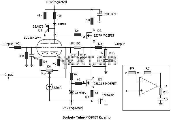
This article discusses several opamp-based headphone amplifier circuits, including suggestions for selecting opamps, input coupling and filtering, high current output stages and power supply options. There are no recommendations for specific opamp brands or models. For tube devotees, there...
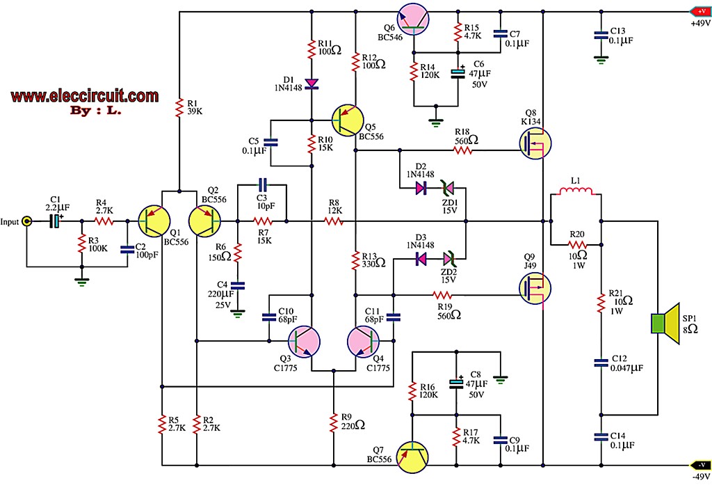
This is the first MOSFET power amplifier designed, featuring a comprehensive circuit. As a 60-watt power amplifier, it is adequate for typical usage. The 60-watt MOSFET power amplifier circuit is designed to deliver high efficiency and robust performance for audio...
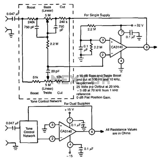
This circuit utilizes the high slew rate, high input impedance, and high output-voltage capability of the CA3140 BiMOS operational amplifier. It also offers mid-band unity gain using standard linear potentiometers. The circuit design leverages the characteristics of the CA3140 BiMOS...
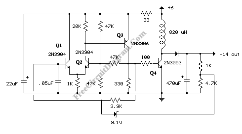
A DC-to-DC step-up converter is typically implemented using a transformer, which converts DC voltage to AC voltage, steps it up with the transformer, and then rectifies and filters the output to achieve a higher DC voltage. However, a voltage...

This differential amplifier utilizes a CA3193 BiMOS operational amplifier. It serves as a classical differential input-to-signal-ended output converter, which, when paired with a low-resistance signal source, will sustain a high common-mode rejection ratio (CMRR), provided that R1 equals R3...