
triggering circuit

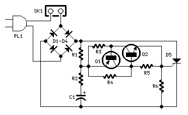
The circuit utilizes a combination of resistors and diodes to efficiently control the operation of SCRs, which are semiconductor devices used for switching and controlling power. The resistor in the circuit serves as a gate drive, providing the necessary current to activate the SCR. The performance of the circuit is heavily influenced by the sensitivity of the SCR's gate; higher sensitivity allows for higher resistance values, while lower sensitivity necessitates lower resistance and higher power ratings to ensure reliable operation.
In the illustrated half-wave circuit, the diode (D1) plays a crucial role by blocking any reverse voltage that could potentially damage the SCR during the negative half-cycle of the AC waveform. This protection is vital for maintaining the integrity of the circuit and ensuring that the SCR only receives the intended forward voltage. The design must account for the peak voltage of the AC supply, which requires careful selection of the diode and resistor ratings to prevent component failure.
The phase control achieved by this circuit enables the adjustment of power delivered to the load by varying the timing of the SCR's triggering relative to the AC supply waveform. This characteristic is particularly useful in applications such as light dimming, motor speed controls, and heating elements, where precise control over power delivery is essential. The ability to modulate the SCR's conduction angle from full-on to half-on allows for smooth transitions and efficient operation across a wide range of applications. Proper thermal management and component selection are also critical to ensure that the circuit operates reliably within the specified temperature range, further enhancing its performance and longevity in practical applications.Simple resistor, diode combinations trigger and control SCRs over the full 180 electrical degree range, performing well at commercial temperatures. These types of circuits operate most satisfactorily when SCRs have fairly strong gate sensitivities. Since in a scheme of this type a resistor must supply all of the gate drive required to turn on the SCR, the less sensitive the gate, the lower the resistance must be, and the greater the power rating. Figure 1 shows a very simple variable resistance half-wave circuit. It provides phase retard from essential zero (SCR full on ) to 90 electrical degrees of the anode voltage wave (SCR half on ).
Diode D1 blocks reverse gate voltage on the negative half-cycle of anode supply voltage. It is necessary to rate blocking to at least the peak value of the AC supply voltage and the trigger voltage producing the gate current to fire IGF are in phase. When EAC = Em, at the peak of the AC supply voltage, the SCR can still trigger with the maximum value of resistance between anode and gate.
🔗 External reference
Related Circuits
This system operates on the principle that the capacitance loading of an oscillator will lower its frequency. When a foreign body comes into contact with the touch plate, the frequency of U1 is lowered. This removes the oscillator signal...
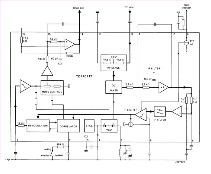
The TDA7021T integrated radio receiver circuit is designed for portable radios, both stereo and mono, where minimal peripheral components are essential for achieving small dimensions and low cost. It is fully compatible. The TDA7021T is a highly integrated radio receiver...
This is a 220V LED flasher circuit designed as a reliable alternative to thermally activated switches used for flashing Christmas tree lamps. It is a cost-effective and easy-to-assemble circuit. The components include R1 (100K), R2 (1K), R5 (1K), R3...
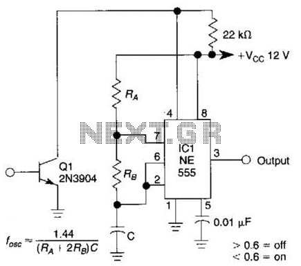
This gated 1-kHz oscillator provides press-to-turn-off functionality, along with waveforms available at the output of pin 3 and across capacitor C1. The gated 1-kHz oscillator circuit is designed to generate a square wave output at a frequency of 1 kHz....

The TDA8358J application circuit is designed for television signal processing. The input signals are connected to the TDA8358J at pins 1 and 2, where pin 1 receives a positive sawtooth voltage input and pin 2 receives a negative sawtooth...

Automatic color holiday lights circuit The automatic color holiday lights circuit is designed to control the operation of decorative lights during festive seasons. This circuit typically utilizes a microcontroller or a timer to manage the sequencing and color changes...