
Variable-Voltage Reference Source

The described circuit is a non-inverting amplifier configuration using an operational amplifier. In this setup, the non-inverting input (positive terminal) is connected to ground, establishing a reference point for the inverting input (negative terminal). The gain of the circuit is controlled by the feedback resistor R2 and an additional resistor R, forming a voltage divider that determines the feedback ratio.
The gain (Av) of a non-inverting amplifier can be expressed as:
\[ Av = 1 + \frac{R2}{R} \]
When R2 is adjusted, the circuit's gain varies accordingly. Setting R2 to zero results in a gain of 1 (unity gain), which implies that the output voltage follows the input voltage closely, producing an output of 0.55 V. This is useful in applications where a buffered output is required without amplification.
On the other hand, increasing R2 to its maximum value allows the circuit to achieve a gain of 50. This configuration amplifies the input signal significantly, yielding an output voltage of approximately 25 V, which is suitable for driving loads that require higher voltage levels.
The circuit is designed to provide stable output regulation, making it effective for applications where a consistent voltage is necessary. The ability to supply several milliamps of output current indicates that this amplifier can drive small loads without significant voltage drop or distortion.
However, one limitation of this circuit is the lack of temperature compensation for the output voltage. Variations in temperature can affect the performance of the op-amp and the resistors, potentially leading to drift in the output voltage. To mitigate this issue, additional components such as temperature sensors or compensation networks may be considered in more critical applications where output stability is paramount. The noninvertiiig terminal of the op amp is grounded, and the circuit uses the voltage at the inverting t erminal as a reference. Its voltage gain is determined by the R2/R ratio. When R2 is set at zero, the circuit has unity gain and a 0.55-V output. When R2 is set to the maximum value, the circuit has a gain of 50 and an output of about 25 V. The circuit provides good regulation and can supply output currents of several milliamps. The output voltage however, is not temperature compensated.
Related Circuits
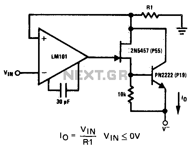
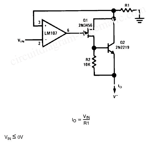
The 2N5457 and PN2222 bipolar transistors function as voltage isolation devices between the output and the current sensing resistor, Rl. The LM101 operational amplifier offers a significant amount of loop gain to ensure that the circuit operates as a...
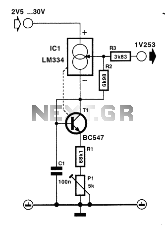
The voltage reference circuit detailed below is a specialized implementation of the LM334 current source. It is characterized by a very low temperature coefficient for the output voltage and consumes only 10 µA at room temperature. This current may...
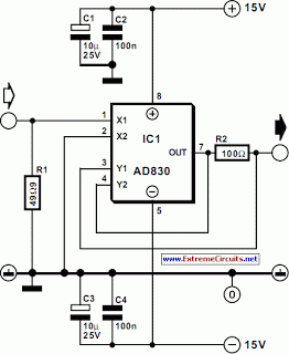
The current source in the diagram reacts very quickly to changes in the input signal and may be utilized in specific measurements. The differential amplifier IC1 ensures that the voltage across resistor R2 is equal to the input voltage,...
The impedance of these current generators is essentially infinite for small currents, and they maintain accuracy as long as VIN is significantly greater than VOS and IO is much higher than I bias. The source employs a FET to...
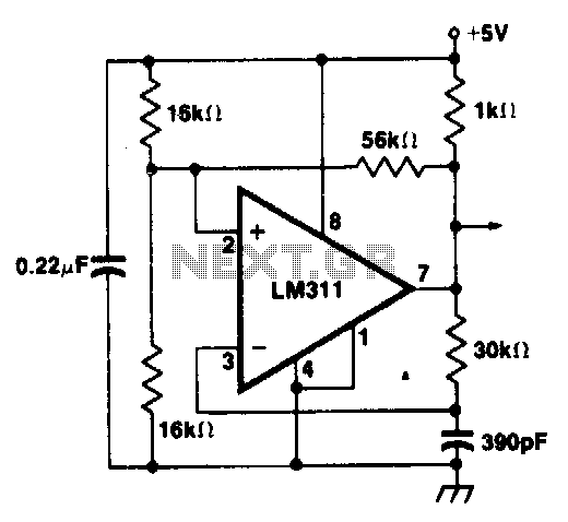
A clock source using the LM311 voltage comparator in positive feedback mode to minimize clock frequency shift problems. The proposed circuit utilizes the LM311 voltage comparator configured in a positive feedback arrangement to generate a stable clock signal. The LM311...

This circuit is designed as a low-cost voltage reference. Its main component is a general-purpose operational amplifier, the 741, configured to output a buffered fixed reference voltage for use by other integrated circuits or circuits, such as an Analog-to-Digital...