
low cost buffered voltage reference

The voltage reference circuit utilizes the operational amplifier 741 in a non-inverting configuration to amplify the reference voltage provided by the AD589. The operational amplifier is powered by a dual supply, typically ±15V, ensuring adequate headroom for the output voltage swing. The AD589, being a bandgap reference, is chosen for its stability over temperature variations and low output drift, making it suitable for precision applications.
In the circuit, the resistors connected to the inverting input of the operational amplifier are configured to set the gain. The resistor values of 1KΩ and 3KΩ create a voltage divider that determines the gain of the operational amplifier. The gain can be calculated using the formula:
\[ \text{Gain} = 1 + \frac{R_f}{R_{in}} \]
where \( R_f \) is the feedback resistor (3KΩ) and \( R_{in} \) is the resistor connected to the inverting input (1KΩ). This results in a gain of approximately 4, which amplifies the 1.23V reference voltage to approximately 4.92V.
The output voltage of the operational amplifier is further buffered to provide a stable 5V reference voltage, suitable for powering other components such as ADCs. The circuit design ensures low output impedance, enhancing the ability to drive loads without significant voltage drop. Additionally, bypass capacitors may be included at the power supply pins of the operational amplifier to filter out noise and improve stability.
Overall, this low-cost voltage reference circuit is effective for applications requiring a stable reference voltage, providing a practical solution for various electronic designs.This is design circuit for a low-cost voltage reference circuit. Its main component is a general-purpose operational amplifier, the 741, configured to output a buffered fixed reference voltage for use by other IC`s or circuits, such as an Analog-to-Digital Converter (ADC). This is the figure of the circuit; The reference circuit above is designed t o output 5 volts, and employs an AD589 as the 741`s own reference. The AD589 is a low-cost, temperature-compensated bandgap voltage reference that provides a constant output of 1. 23 V. Thus, the voltage at both inputs of the 741 is 1. 23 V, which is also the voltage at the junction of the 1K and 3K resistors connected to the inverting input.
This forces the 741 to output a steady voltage of approximately 5V (1. 23V x 4K/1K = 4. 92V). 🔗 External reference
Related Circuits
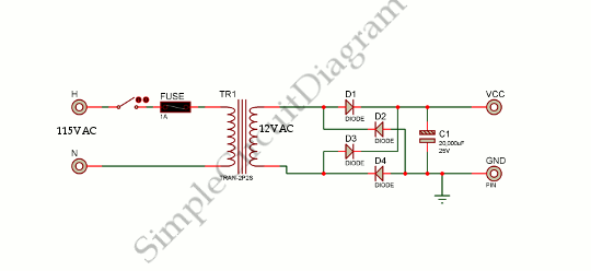
This is a power supply circuit that produces a voltage range of 12 to 24 V. It is straightforward, requiring only a bridge rectifier, a filter capacitor, and a transformer, without the need for a regulator. A bridge rectifier...
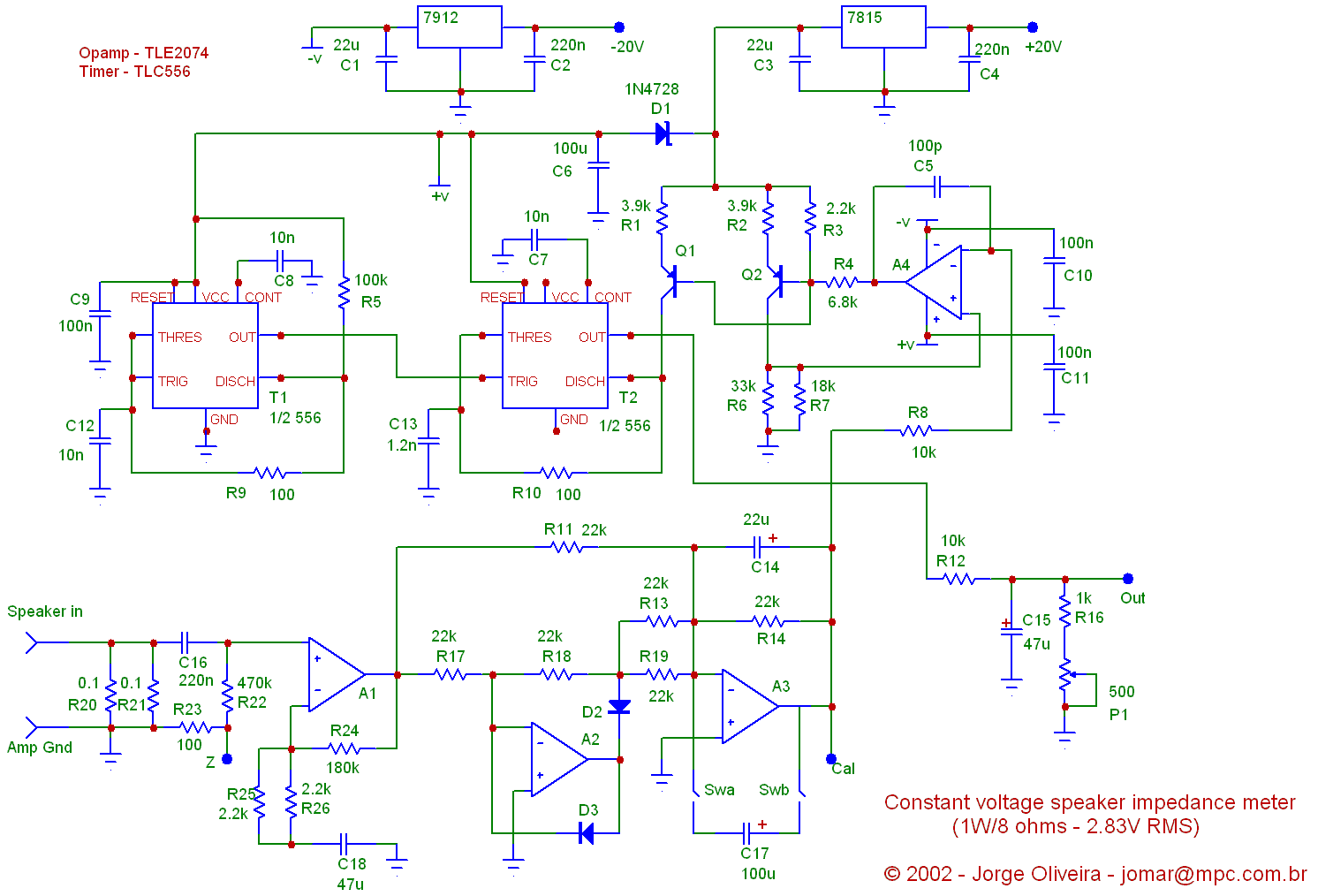
If the offset value exceeds 5mV, adjust this value by experimenting with resistors, starting with 220K, connected from test point Z (the junction of R22 and R23) to +V if there is a negative voltage, or to -V if...
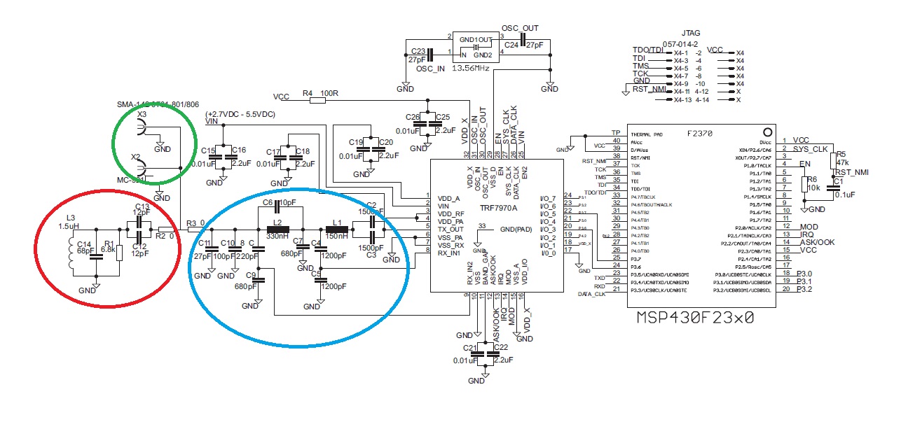
The "green area" is designated for the placement of the TRF7970A's antenna, which should be connected between two 0-ohm resistors. The antenna can be constructed step by step following the guidelines in the document "Antenna Matching for the TRF7960...

Most small internal combustion engines used in model building utilize glow plugs for starting. However, glow plugs operate at 1.5 V, while components like fuel pumps, starter motors, and chargers typically operate at 12 V. This discrepancy necessitates a...
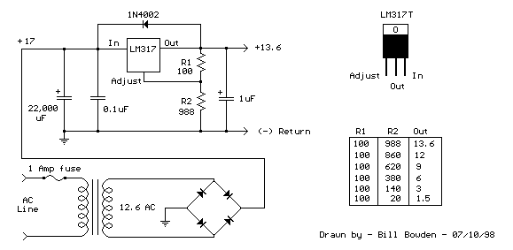
The LM317T is an adjustable three-terminal positive voltage regulator capable of supplying more than 1.5 amps with an output range of 1.25 to 37 volts. The device features built-in current limiting and thermal shutdown, making it robust against failure....
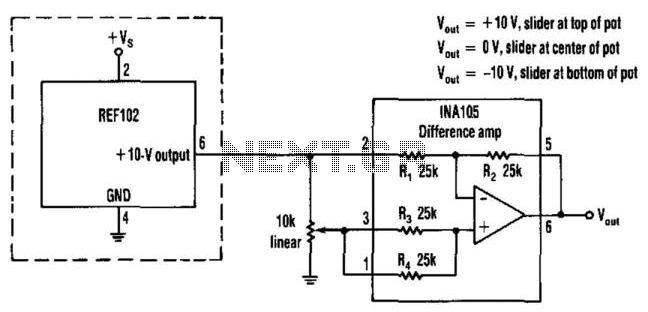
This circuit provides a precision voltage source that can be adjusted to produce zero, positive, and negative voltages, eliminating the need to reverse connections on the power supply. It allows for achieving exactly 0 V without any offset. The...