
Voltage-Controlled Amplifier

The CA3080 operational amplifier is designed for applications requiring variable gain control. In this configuration, the resistors R1 and R2 form a voltage divider that sets the input signal level to a manageable 20 mV peak-to-peak, ensuring that the amplifier operates within its linear region and avoids distortion. When the input signal exceeds this level, the output may exhibit nonlinear characteristics, which can be beneficial in specific applications like waveform shaping.
The gain control is achieved through the IABC current, which is injected into pin 5 of the CA3080. The relationship between IABC and the gain is critical; as IABC increases from 0.1 mA to 1 mA, the gain increases linearly, allowing for precise control over the output signal. This feature is particularly useful in applications where dynamic range and signal integrity are paramount.
The output of the CA3080 is a current that must be converted to a voltage for practical use. This is accomplished by connecting the output to a resistive load, R5, which converts the current output to a voltage output according to Ohm's law (V = IR). The output impedance at pin 6 is specified at 10 kΩ, which can lead to loading effects if not properly managed. To mitigate this, a voltage follower (IC2) is employed to provide a low output impedance, ensuring that the subsequent stages of the circuit receive a stable voltage without being affected by variations in load.
The precision voltage-to-current converter circuit around IC3 plays a crucial role in generating the IABC current. This converter allows for fine adjustments to the gain by varying the control voltage Vm. A positive Vm results in a proportional increase in IABC, thereby increasing the gain, while a negative Vm effectively reduces IABC to zero, disabling the gain altogether. This dual functionality enables versatile applications in signal processing, where both amplification and attenuation may be required. Overall, the CA3080's design and capabilities make it an effective component for analog signal manipulation in various electronic circuits. The CA3080 can be used as a gain controlling device. The input signal is attenuated by R1/R2 so that a 20-mVpp signal is applied to the input terminals. If this voltage is much larger, significant distortion will occur at the output. In fact, this distortion is put to good use in the triangle-to-sine wave converter. The gain of the circuit is controlled by the magnitude of the current IABC. This current flows into the CA3080 at pin 5, which is held at one diode voltage drop above the - VCc rail· The gain of the CA3080 is " "linearly" proportional to the magnitude of the IABC current over a range of 0.1 to 1 mA. Thus, by controlling IABC, you can control the signal level at the output. The output is a current output, which has to be "dumped" into a resistive load (R5) to produce a voltage output.
The output impedance at IC1 pin 6 is 10 kfi (R5), but this is "unloaded" by the voltage follower (IC2) to produce a low output impedance. The circuit around IC3 is a precision voltage-to-current converter and this can be used to generate IABC.
When Vm (control) is positive, it linearly controls the gain of the circuit. When it is negative, IABC is zero and so the gain is zero.
Related Circuits
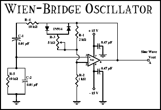
The Wien-Bridge oscillator meets specific requirements due to the presence of a low-pass filter, a high-pass filter, and a 180-degree phase shift from the feedback networks connecting the input to the output. This configuration results in a total phase...
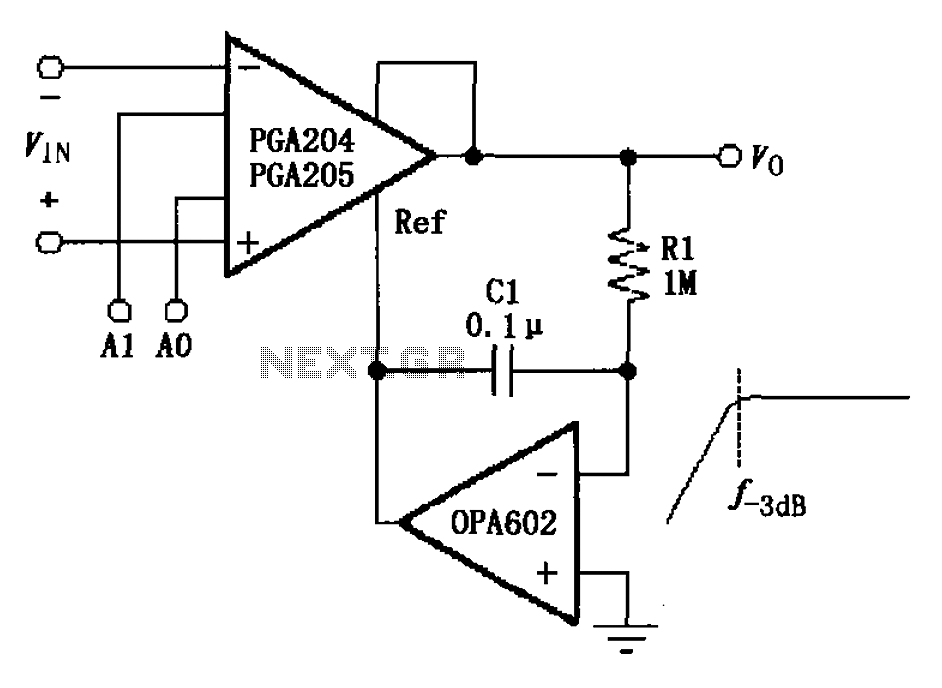
The circuit depicted in the figure features a programmable amplifier utilizing the PGA204/205 operational amplifiers in conjunction with the OPA602. The OPA602 op-amp is configured to establish a feedback reference point, while external components, specifically the capacitor C1 and...
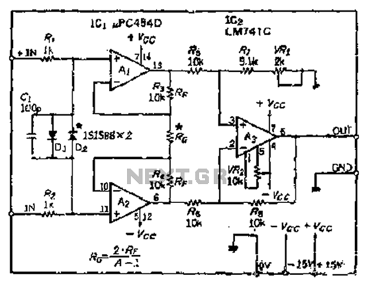
All resistance values are equal, resulting in the Cantonese operational amplifier's gain (A) being equal to 1. However, by selecting smaller resistances, the gain can be adjusted. The circuit can achieve the desired gain through six configurations. Two heavy...
SW1 bypasses the crossfeed network. I have reconfigured the original crossfeed schematic so that now the 100k resistor always bridges the bypass switch and thereby reduces any 'crackle' or 'click' or whatever you may call them. Don't omit these...

The TDA7381 is a Class AB audio power amplifier housed in a Flexiwatt25 package, specifically intended for car radio applications. This circuit can also be utilized for various other purposes. The fully complementary PNP/NPN output configuration enables a rail-to-rail...
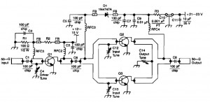
This RF amplifier circuit delivers a power output of 4 Watts at a frequency of 900 MHz. It utilizes Wilkinson power dividers in the base and collector circuits of transistors Q2 and Q3. Two SD1853 driver application transistors are...