
Voltage-to-current converter

The described circuit operates on the principle of current sensing and regulation, where the output current (Iqut) is determined by the input voltage (Vin) divided by a resistance (R). This configuration is typically used in applications requiring precise current control. The use of a PNP transistor allows for the management of negative currents, which is essential in certain circuit designs where the load may require reverse polarity operation.
In scenarios demanding higher current accuracy, substituting the standard PNP transistor with a Darlington pair is advisable. A Darlington pair consists of two bipolar junction transistors (BJTs) connected in such a way that the current amplified by the first transistor is fed into the second transistor, resulting in a significant increase in current gain. This configuration enhances the sensitivity and accuracy of the current sensing mechanism, making it suitable for applications where precision is paramount.
To ensure stability and prevent oscillations in the circuit, unity gain compensation is required. This involves adding a compensation capacitor in the feedback loop to maintain a stable gain across the operational range. The capacitor's value must be carefully calculated based on the circuit's frequency response and load conditions to achieve the desired performance without introducing phase shifts that could lead to instability.
Overall, with meticulous design considerations, this circuit can effectively manage high currents while maintaining accuracy and stability, making it a valuable component in various electronic applications such as power supplies, motor controllers, and current regulators.The current out is Iqut—Vin/R. For negative currents, a PNP can be used and, for better accuracy,-a Darlington pair can be substituted for the transistor. With careful design, this circuit can be used to control currents of many amps Unity gain compensation is necessary.
Related Circuits
Both converters utilize CMOS inverters. Figure 105-1A illustrates a free-running circuit where both pulse duration and pulse pause are influenced by the temperature of diode D8. This configuration is suitable for applications where synchronization between the converter and other...

A low-power converter designed to derive a higher voltage from a main system rail in an on-board application. The operating frequency with the transformer depicted is 250 kHz. Z1 functions as a dissipative voltage regulator for the output and...
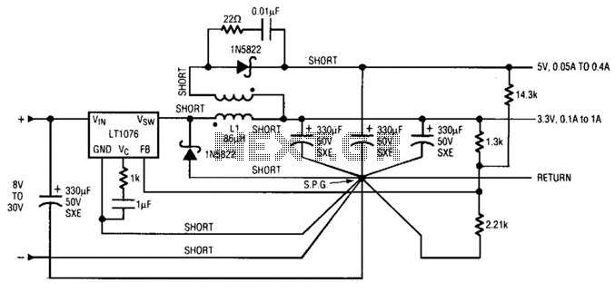
Input voltages can range from 8 V to 30 V. The load range for the 5 V output is from 0.05 A to 5 A, while the load range for the 3.3 V output is from 0.1 A to...
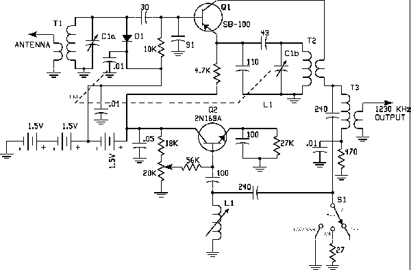
The 1956 Regency ATC-1 converter marked the beginning of a new era in amateur radio. This compact converter utilized only two transistors—one PNP and one NPN—both made of germanium and now considered obsolete. However, they represented the onset of...
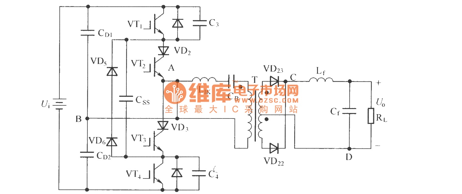
To eliminate circulating current in a zero-voltage switch three-level DC converter during its zero state, a zero-voltage zero-current switch three-level DC converter circuit has been proposed. The primary distinction between this circuit and the standard zero-voltage switch three-level DC...
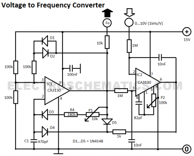
This voltage-to-frequency converter circuit features a voltage-controlled oscillator with a small deviation of 0.5%. The integrated circuit IC1 operates as a multivibrator. The voltage-to-frequency converter circuit is designed to convert an input voltage into a corresponding frequency output. The core...