
The pulse width detection circuit 555
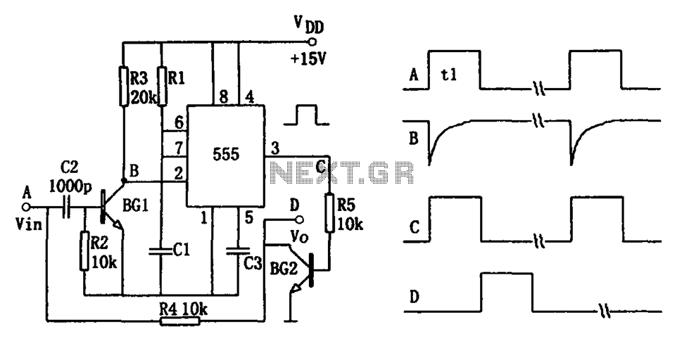
The pulse-width detection circuit serves to identify and measure the duration of input pulse signals, making it essential in various applications such as signal processing and timing analysis. The differential circuit, comprising resistors R2 and capacitor C2, functions to amplify the input pulse signal while filtering out noise, ensuring that only the relevant pulse characteristics are processed. The operational amplifier BG1 enhances the signal further, providing a clean representation of the input wave.
The 555 timer, configured in a monostable mode, is critical for generating a consistent output pulse in response to the input signal. Its timing characteristics are determined by the resistor R1 and capacitor C1, establishing the pulse width td. This configuration allows for precise control over the timing, making it adaptable for different applications by simply adjusting R1 and C1 values.
The transistor BG2 acts as a switch, responding to the output from the 555 timer. When a pulse is detected that exceeds the set width, BG2 remains in a conductive state longer than the pulse duration, which is indicated by a high output at V0. This functionality is crucial for applications requiring pulse width modulation or timing detection, allowing for effective monitoring and control of signal durations in electronic systems.
Overall, this pulse-width detection circuit is a robust solution for analyzing pulse signals, with its modular components allowing for flexibility and customization based on specific requirements.As shown in Fig pulse-width detection circuit. The detection circuit by the differential circuit (R2, C2), amplifier BG1, single stabilizing circuit (555, R1, C1) and other components. Pulse signal Vin (such as a wave A) all the way to add to the input differential amplifier circuit, another path R4 is added to the collector circuit BG2. By the negative-going pulses (such as waveform B) trigger circuit 555 is set to a certain output pin positive pulse width (such as waveform C) after the differential amplifier, which is the one-shot pulse circuit timing td 1.1 R1C1 (seconds), and the positive pulse is applied to the base of BG2, so during detection, BG2 saturated conduction, the collector (ie, the circuit output V0) was low.
If they are detected pulse width greater than the set width td, due to the collector BG2 pressing for longer than the base bias time td, V0 appear high, indicating that the detected pulse width exceeds a set time.
Related Circuits
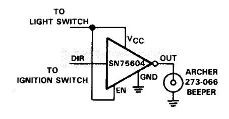
The SN75604, which features input control logic and requires only a single supply rail, can be utilized in light activation sensors and alarm drivers. The device's Vqq and enable inputs are connected to a voltage lead from the light...
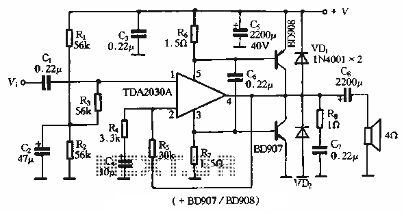
The rDA2030A TDA2030 is an enhanced version of the original product, with a maximum working voltage increased to 18V and a maximum output power of 18W. Additionally, harmonic distortion has been significantly reduced. The application circuit is illustrated. The rDA2030A...
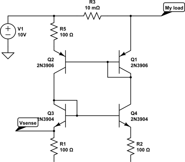
The bases and emitters of the transistors are connected together, resulting in equal base-emitter voltages. Assuming the transistors are identical, equal Vbe leads to equal base currents, which in turn results in equal collector-emitter currents. By adjusting the voltage...
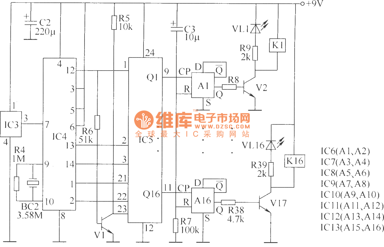
The wireless remote control transmitter circuit consists of control buttons S1 to S16, resistors R1 to R3, a capacitor C1, a regulator diode VS, a crystal oscillator BC1, and DTMF encoder integrated circuits IC1 and IC2. The circuit components...
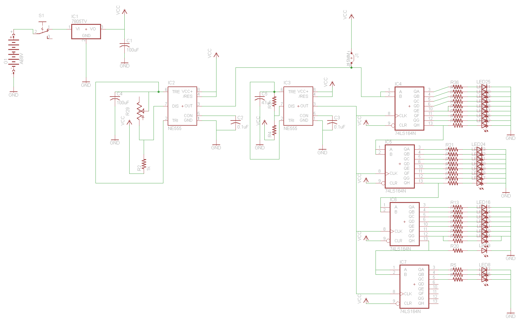
For the two-layer board schematic, six core integrated circuits (ICs) will be utilized: four 74LS164 shift registers and two 555 timers. The schematic will be constructed using the Eagle Layout Editor, as all required components are available in its...
The DC voltage for the generator field winding is supplied by a three-phase thyristor rectifier. In instances of incorrect operation, phase misalignment, or system failure, the rectifier may generate hazardous conditions, leading to over-voltage insulation issues on the DC...
Warning: include(partials/cookie-banner.php): Failed to open stream: Permission denied in /var/www/html/nextgr/view-circuit.php on line 713
Warning: include(): Failed opening 'partials/cookie-banner.php' for inclusion (include_path='.:/usr/share/php') in /var/www/html/nextgr/view-circuit.php on line 713