
Optocouplers and transistors of the bistable circuit diagram

The bistable circuit described operates based on the principles of feedback and optical isolation provided by the optocoupler. The circuit employs a transistor (VT) that serves as a switching element, which can toggle between two states: on and off. The initial state of the circuit is defined when the supply voltage is applied, at which point VT is off, resulting in a high output potential.
When a forward pulse signal is applied to the input terminal, it triggers an increase in the collector current of VT. This increase activates the optocoupler's light-emitting diode, which emits light that is detected by the phototransistor. The phototransistor's response reduces its collector-emitter resistance, allowing more base current to flow into VT. This feedback loop amplifies the base current, driving VT into saturation rapidly, which flips the output from high to low.
In the case of a negative pulse, the process reverses. The decrease in collector current causes the LED of the optocoupler to dim, which in turn reduces the base current of VT. The reduction in base current further decreases the collector current, leading to a swift turn-off of VT. As a result, the LED turns off, the phototransistor becomes inactive, and VT stabilizes in the off state, shifting the flip-flop back to a high output state.
This bistable configuration is particularly advantageous due to its resilience to noise, making it suitable for applications where signal integrity is critical. The use of an optocoupler provides electrical isolation between the input and output, enhancing the circuit's robustness against external disturbances. Overall, the design effectively leverages feedback mechanisms and optical components to create a reliable bistable switching circuit. As shown by the bistable circuit and optocoupler transistor of FIG. In the initial state the moment the supply voltage is turned on, the transistor VT off, the circuit outputs a high potential. When the input terminal with a forward pulse, so that the collector current increases VT, optocoupler light emitting diode, phototransistor collector-emitter resistance among smaller, resulting in VT base current increases, the formation of positive feedback, so fast VT saturation, from 1 to 0. When you enter a negative pulse, VT collector current decreases, thereby enabling VT darken the light emitting diode base current decreases, causing VT collector current is further reduced, so that VT quickly turned off, and the light emitting diode does not light, phototransistor is turned off, so that VT stable in the off state, the flip-flop from 0 to l state.
This can improve the anti-jamming capability bistable circuit bistable circuit.
Related Circuits
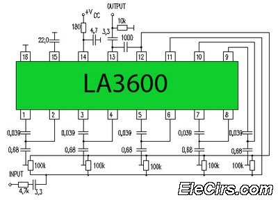
Circuit LA3600 5 Band Equalizer Circuit Schematics. One type of tone control in audio electronics is the graphic equalizer. Graphic equalizers can be categorized into two types: bar and other configurations. The LA3600 circuit is a 5-band graphic equalizer designed...
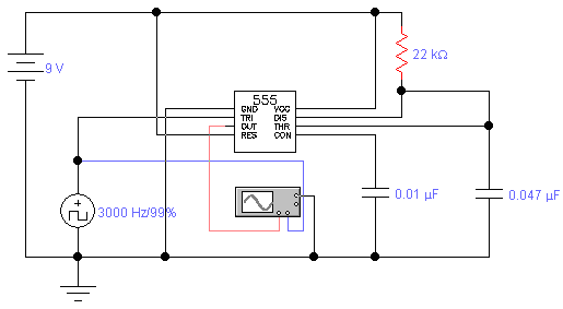
The standard assumption is that the phase shift sections operate independently. According to the equation provided, the loop phase shift reaches -180 degrees when the phase shift of each section is 60 degrees. This condition is met when ω...

The transmitter provides an optical link (infrared) for headphones. Three infrared LEDs (IR) are powered by T1, with P1 used to adjust the current level. The current consumption of this headphones infrared transmitter is approximately 60mA at 9V. The infrared...
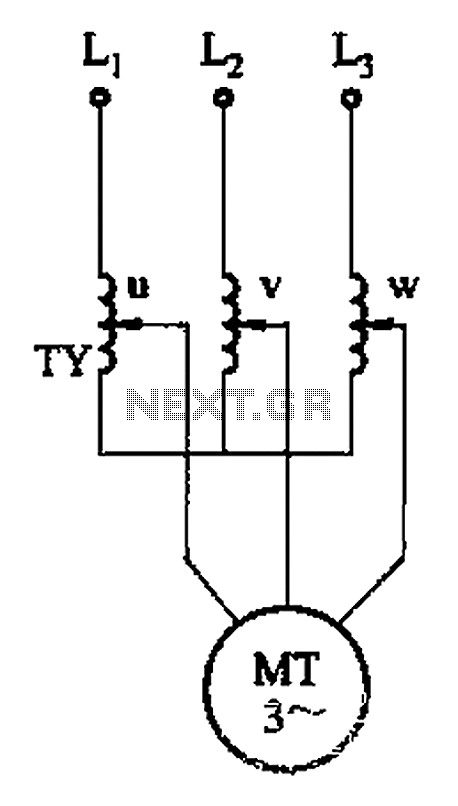
The circuit depicted in Figure 3-176 illustrates an adjustment method that allows the motor to operate at equilibrium. The adjustment range is relatively wide; however, it necessitates a three-phase voltage regulator, which incurs higher input costs. The circuit design in...
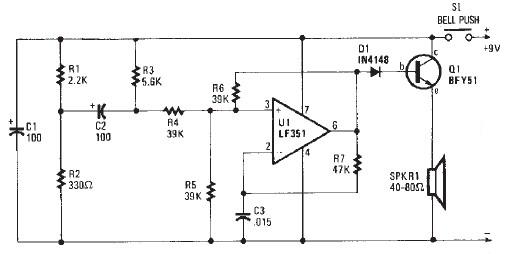
This electronic door buzzer circuit schematic has a straightforward function and is simple to construct. The circuit employs an LF351 operational amplifier along with a few common electronic components. When the S1 push-button is pressed, a positive voltage is...
The metal detector circuit is presented here, illustrating a simple yet effective design. It utilizes a 40, 106 Hex Schmitt inverter IC, a capacitor, a search coil, and batteries. An advantage of connecting IC1b Pin 4 to a medium-wave...