
The triangular wave carrier generator circuit diagram
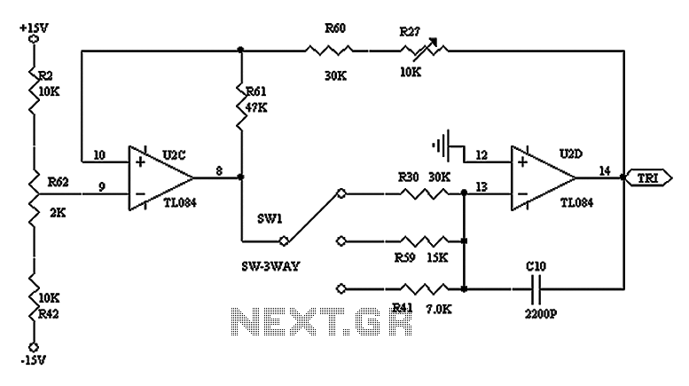
The triangular wave generator circuit described employs two operational amplifiers configured in a feedback loop to produce a stable triangular waveform. The use of operational amplifiers is advantageous due to their high input impedance and low output impedance, which facilitate effective signal processing.
R62, the offset adjustment resistor, plays a crucial role in calibrating the output waveform to ensure that it oscillates symmetrically around a desired voltage level. By adjusting R62, the user can fine-tune the baseline voltage of the triangular wave, accommodating variations in power supply or desired output levels.
R27, the peak adjustment resistor, allows for the modification of the amplitude of the triangular waveform. This adjustment is essential for applications that require specific voltage levels or for interfacing with other circuit components that may have varying input requirements.
The inclusion of a switch to select different resistances enhances the circuit's versatility. By changing the resistance values, the frequency of the output triangular wave can be altered. This feature is particularly useful in applications such as signal modulation, waveform generation for testing purposes, or in audio synthesis where different frequencies are needed.
Overall, this triangular wave circuit is designed for flexibility and precision, making it suitable for various electronic applications where a stable and adjustable waveform is required. As shown by the triangular wave circuit composed of two OP, R62 is OFFSET adjustment, R27 for the adjustment of the peak, with the switch to select different resistance obtaine d triangular waves of different frequencies.
Related Circuits
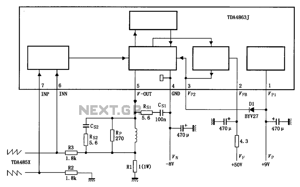
The TDA4863J basic application circuit operates with a positive supply voltage (VP), a flyback power supply voltage (VF), and a negative supply voltage (VN). The input signal is provided from the sawtooth signal input at pins 6 and 7,...
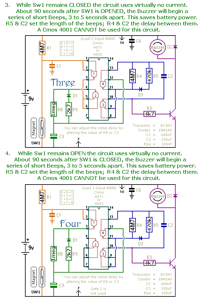
This document presents a collection of compact, self-contained alarm circuits. These circuits are designed to operate with a very low standby current, making them ideal for battery-powered applications. They can be triggered by both normally-open and normally-closed switches, while...
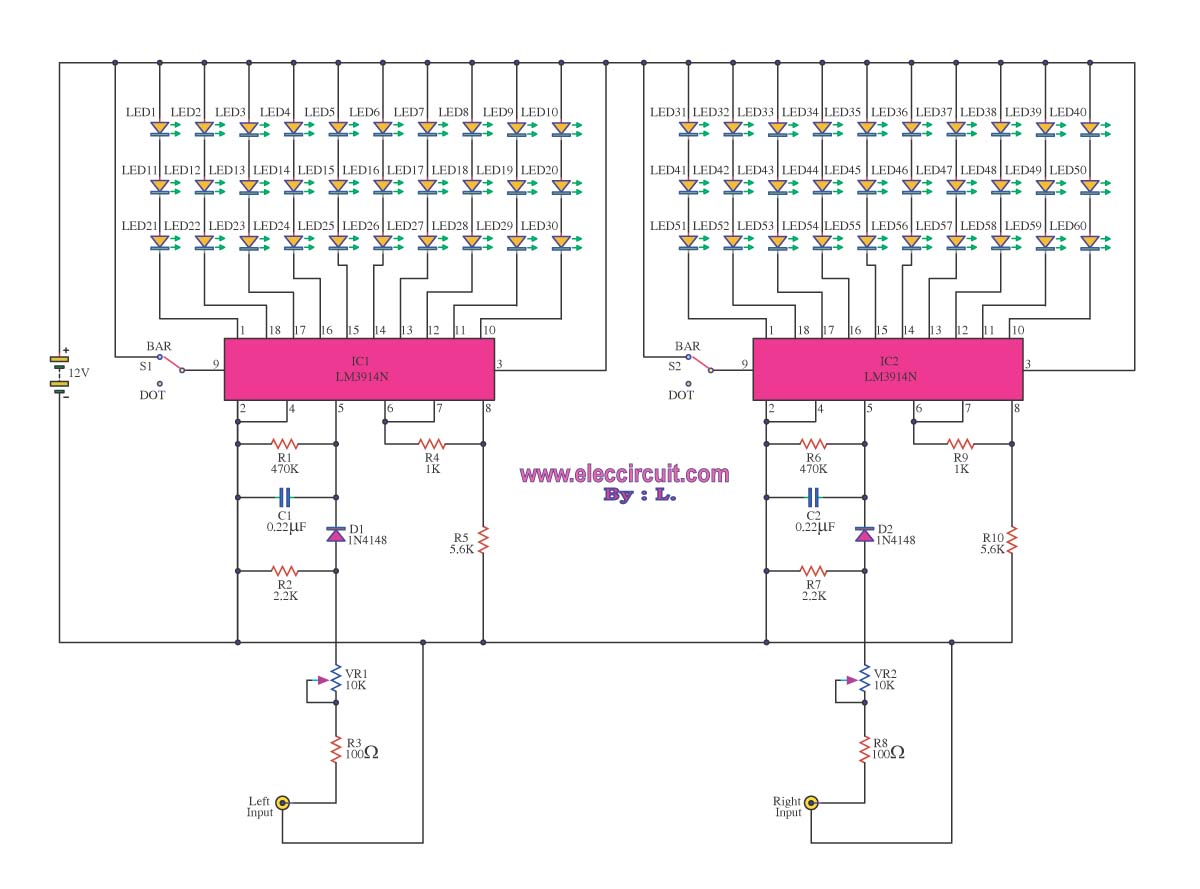
A VU meter is utilized to display the power level of audio signals and also serves as an aesthetic element. When purchasing a VU meter kit from an electronics store, options include assembling various parts independently or selecting a...
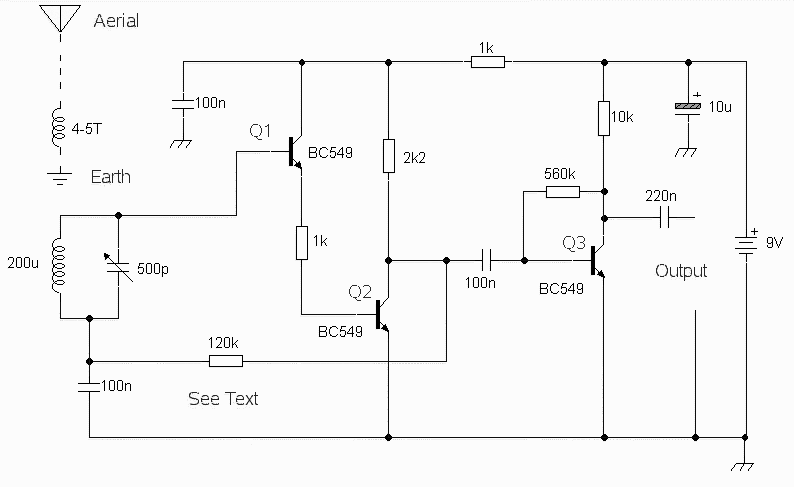
The circuit was designed to obtain signals through amplitude modulation, exhibiting good sensitivity and selectivity. Amplitude modulation. The amplitude modulation (AM) circuit is engineered to effectively capture and process radio frequency signals. The design focuses on achieving high sensitivity, allowing...
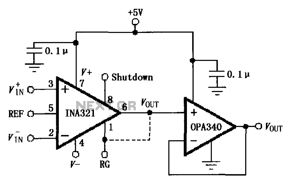
The circuit depicted in the figure consists of an OPA340 operational amplifier configured as a voltage follower, serving as an output buffer for the INA321/322 output. The optimal load impedance for the INA321/322 is 10k ohms or greater. A...
This small device is designed to jam remote controls by directing it at the TV. The circuit utilizes a 555 timer configured as an astable multivibrator, generating a frequency of approximately 38 kHz, which corresponds to the frequency at...
Warning: include(partials/cookie-banner.php): Failed to open stream: Permission denied in /var/www/html/nextgr/view-circuit.php on line 713
Warning: include(): Failed opening 'partials/cookie-banner.php' for inclusion (include_path='.:/usr/share/php') in /var/www/html/nextgr/view-circuit.php on line 713