
TDA4863AJ Basic Application Circuit a
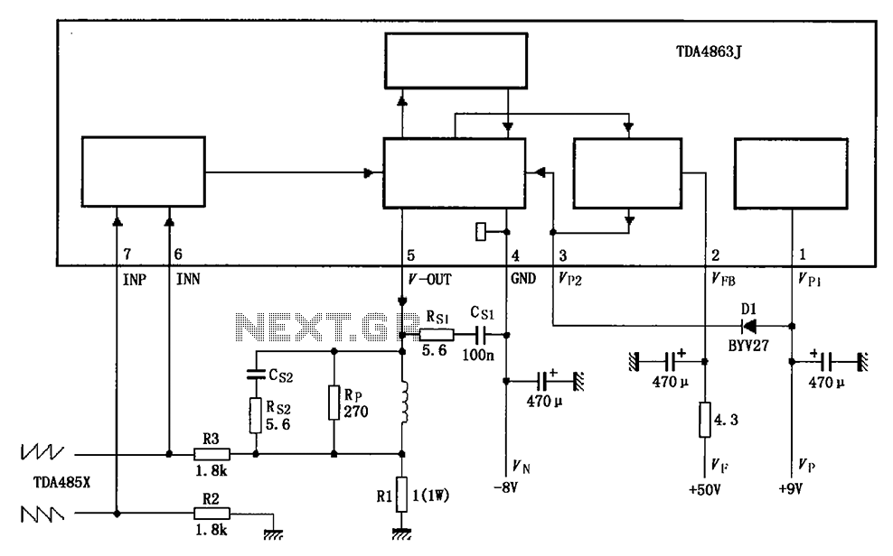
The TDA4863J circuit is designed for efficient vertical deflection in display applications, utilizing a combination of voltage supplies to manage the operational requirements. The differential input stage is crucial for processing the sawtooth signal, which is fundamental for generating the vertical deflection required for raster scanning in cathode-ray tube (CRT) displays or similar technologies.
The push-pull output stage enhances the performance of the vertical output by providing sufficient current to drive the deflection coils, which are responsible for directing the electron beam across the screen. The sawtooth waveform produced is tailored to ensure that the beam moves smoothly and accurately, with the retrace generator playing a vital role in minimizing power consumption during the non-active scanning period.
Temperature protection mechanisms are essential for maintaining the reliability of the circuit. The inclusion of a temperature sensor (T1) allows for real-time monitoring of the vertical output stage's thermal conditions. If the temperature exceeds the threshold, the circuit intelligently reduces the output current, preventing potential thermal damage to the TDA4863J chip.
The choice of capacitor Cs2 at 150nF is a critical design parameter, affecting both the retrace time and the noise performance of the circuit. Proper selection of this component ensures that the circuit operates within optimal parameters, delivering high-quality output while minimizing interference. Overall, the TDA4863J circuit exemplifies a well-engineered solution for managing vertical deflection in electronic displays, balancing performance, efficiency, and safety. As shown for the TDA4863J basic application circuit. When the positive supply voltage VP, VF flyback power supply voltage and a negative supply voltage VN to work together with the circuit, the input signal from the sawtooth signal input 6 feet and 7 feet to the inside of the differential input stage of the inverting input terminal and inverting input terminal, the output from the vertical output stage 5 feet after sawtooth voltage amplification. Wherein, subject to the vertical complementary push-pull output stage output amplifier, the sawtooth voltage of the power amplifier, a sawtooth deflection current produces a magnetic field required for imaging through the deflection coils controlling the electron beam scans linearly.
During retrace, retrace generator to supply power to the vertical output stage, so as to have minimal power consumption in a short retrace time. Vertical output stage has a temperature limit protection, when T1 150 starts to decrease when the vertical output stage output current to protect the chip, so that will not overheat and damage.
Cs2 typical value 150nF, then retrace time and the best noise performance.
Related Circuits
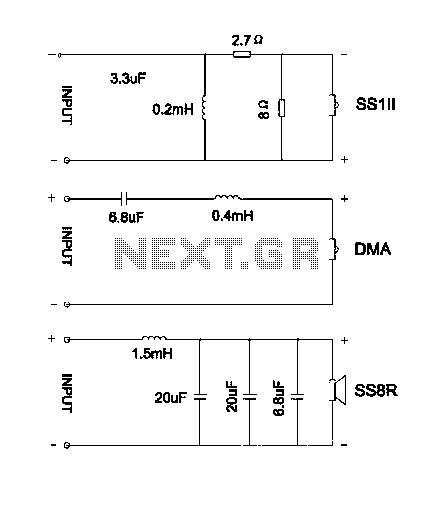
The divider acts as the speaker's brain and is crucial for sound quality. The music amplifier's output signal must be processed through a wave filter element to divide it into specific frequency signals for each unit. A scientifically and...
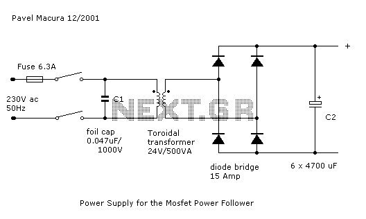
The circuit comprises an N-MOSFET voltage follower (T1, common drain) and a current source (T2, NPN Darlington). The current source is set to 2.2 Amps. With a supply voltage of 40V, the circuit can deliver approximately 17W into an...
The current design of a power inverter offers an efficiency of approximately 85% and a power output exceeding 200 watts. This document provides a complete circuit schematic and detailed building procedure for a home-built power inverter. While numerous articles...
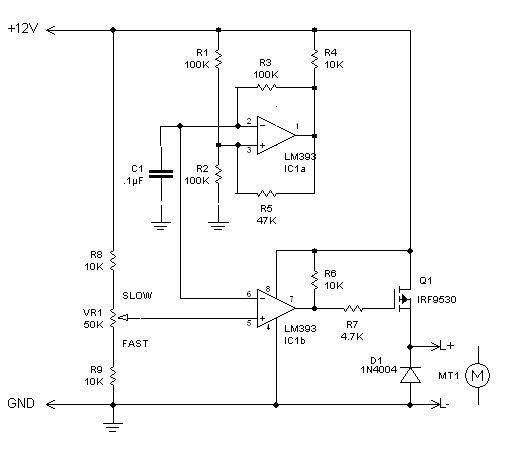
The inquiry pertains to identifying the component within the circuit that regulates the minimum RPM achievable. The current operational range of the motor is between 1400 and 3700 RPM, and there is an interest in modifying the circuit to...

The LK16-5/31 type master controller and PQY2 Series Magnetic control panel comprise a control circuit. The PQY2 series control panel, along with the magnetic PQY1 control panel, features a similar control circuit. The electrical components are fundamentally the same;...
The circuit for automatic brightness adjustment in a television utilizes a photosensitive resistor and a contrast potentiometer connected to an intermediate stage. The photosensitive resistor varies its resistance based on light intensity, causing changes in the potential at the...
Warning: include(partials/cookie-banner.php): Failed to open stream: Permission denied in /var/www/html/nextgr/view-circuit.php on line 713
Warning: include(): Failed opening 'partials/cookie-banner.php' for inclusion (include_path='.:/usr/share/php') in /var/www/html/nextgr/view-circuit.php on line 713