
PGA202 offset voltage correction circuit

The PGA202 offset voltage correction circuit utilizes a precision instrumentation amplifier, the PGA202, which is capable of providing variable gain settings to accommodate a range of applications. The circuit's design addresses the inherent input and output offset voltages that can affect the accuracy of measurements in sensitive electronic systems.
The gain settings of the PGA202 can be configured through external resistors, allowing for flexibility in signal amplification. The presence of a 50k potentiometer for input offset voltage correction enables fine-tuning of the input stage, ensuring that any offset introduced by the amplifier itself can be minimized. This is particularly crucial in applications where small signal detection is necessary, as even minor offsets can lead to significant errors in output readings.
The output offset voltage calibration is managed through a 10k potentiometer, which allows for adjustments after amplification. This stage is critical for achieving a zero output voltage when no input signal is present, thereby enhancing the overall accuracy of the system. The inclusion of the OPA602 operational amplifier as a voltage follower serves to buffer the output, minimizing the load on the PGA202 and ensuring that the output impedance remains low. This configuration is beneficial for interfacing with subsequent circuitry, as it prevents signal degradation.
For the adjustment process, the connection of a voltmeter to pin 12 provides a direct means to monitor the output voltage. By shorting pins 7 and 8, the input voltage (VIN) is effectively set to zero, establishing a baseline for calibration. The iterative adjustment of the 50k and 10k potentiometers allows the user to achieve a precise zero indication on the voltmeter, confirming that the offset correction has been successfully implemented.
Overall, this circuit exemplifies a well-engineered solution for offset voltage correction, utilizing common electronic components to achieve high precision in measurement and amplification tasks. The careful selection of potentiometer values and the use of a voltage follower ensure that the circuit remains adaptable to various operational conditions while maintaining accuracy. As shown for the PGA202 offset voltage correction circuit. PGA202 offset voltage correction circuits for input offset voltage and output offset voltage is corrected. Since ther e are four kinds PGA202 gain, input offset voltage at different gain slightly different, 50k potentiometer for correcting the input offset voltage; output offset voltage using 10k potentiometer calibration. OPA602 op amp voltage follower composition, low resistance output to 4 feet. Adjustment: at the output connected to a voltmeter 12 feet, 7-8 feet short PGA202 make VIN 0, respectively, and repeatedly adjust 50k 10k potentiometer, so that the output voltage meter to zero indication.
Related Circuits
The circuit principle involves using a current transformer for current sensing due to the large AC power load of computers. This setup detects whether there is current in the power line, enabling the determination of its status. The LM393...
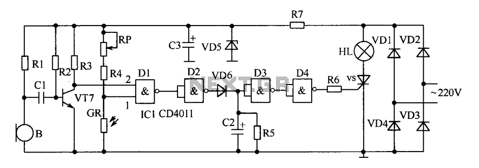
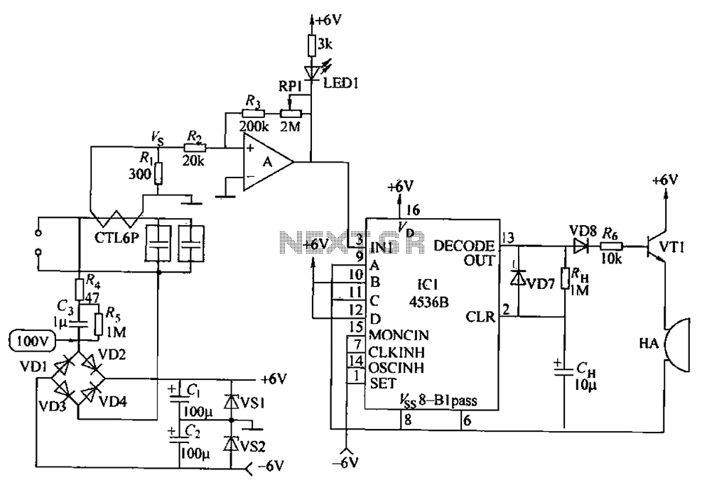
The delay-saving lamp circuit functions as a sound and light control delay energy-saving lighting system. It can directly replace a standard light switch without modifying the existing lighting circuits. In bright or daytime conditions, the sound control feature ensures...
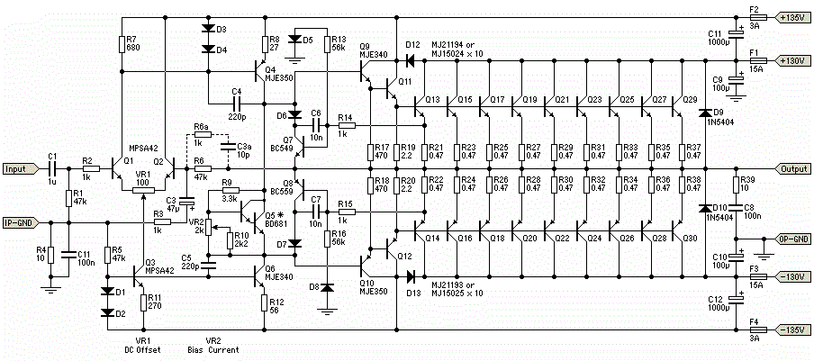
The circuit for the power amplifier has a power output of up to 1500W RMS and is commonly utilized in outdoor sound systems. The final image displays a series of power amplifiers that utilize 10 sets of power transistors....
This quartz crystal oscillator circuit exhibits greater stability compared to a parallel resonance circuit. It is capable of generating frequencies up to 30 MHz or even higher when utilizing BFR91 transistors for T1 and T2, along with reduced values...
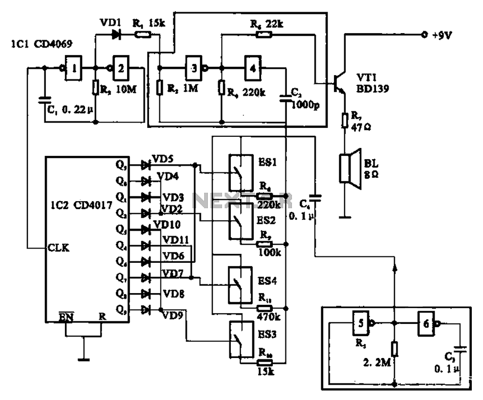
The circuit illustrated is an analog signal generator designed to produce a chirping sound, simulating birds singing. It employs six CD4069 inverters to create three oscillators, with two of them functioning as ultra-low frequency oscillators. The oscillation frequency is...
In electronic technology, the triode utilizes a variety of general components and parts. The parameters of the triode and numerous electrical parametric measurement schemes are closely related to measurement results. Therefore, in electronic design, the base pin, typological judgment,...
Warning: include(partials/cookie-banner.php): Failed to open stream: Permission denied in /var/www/html/nextgr/view-circuit.php on line 713
Warning: include(): Failed opening 'partials/cookie-banner.php' for inclusion (include_path='.:/usr/share/php') in /var/www/html/nextgr/view-circuit.php on line 713