
Basic circuit diagram connection ISO120 121 signals and power supply

The ISO120/121 circuit design emphasizes the importance of proper layout and component placement to ensure signal integrity and minimize noise interference. The use of a 1 µF tantalum capacitor at each power supply terminal serves as a crucial bypass filter, which helps to stabilize the power supply voltage and reduce high-frequency noise. The proximity of these capacitors to the chip is critical, as it minimizes the inductance of the connections and enhances the effectiveness of the bypassing.
In designing the printed circuit board (PCB), it is essential to maintain trace independence to avoid crosstalk and signal degradation. This can be achieved by routing signal traces away from each other and ensuring that they do not share a common ground path, which can introduce noise. The layout should also consider the environmental conditions in which the circuit will operate. In a high-noise environment, careful attention must be paid to the routing of sensitive signals. A high impedance output common area allows for better isolation from noise, ensuring that the integrity of the signals is maintained.
The common ground for bias current return must be designed to maintain a voltage level of at least 1V above the ground level to prevent ground loops and ensure accurate signal transmission. The placement of the sense pin at the load's distal end helps to reduce the impact of voltage drops due to long wire runs, thereby enhancing the accuracy of the measurements.
The C1H and C2H pins, which connect to external integrating capacitors, are integral to the internal integration circuit's summing node. These components are susceptible to external interference, necessitating the implementation of a ground protective ring around them. This ring acts as a shield, reducing the likelihood of interference affecting the sensitive circuitry. By incorporating these design strategies, the circuit can achieve optimal performance and reliability in various operating conditions. As shown for the basic connection circuit ISO120/121 signals and power supply. Each power supply terminal must have a 1 F tantalum capacitor as a bypass filter, printed circuit board layout should be possible to bypass capacitor placed close to the chip. In the design of printed circuit board layout, all the land as independent as possible traces connected to a common end, namely the use of a little ground. When applied in a noisy environment, in order to prevent noise-sensitive signal fleeing, in the design of printed circuit board wiring should be a common input signal and provide a high impedance output common area.
Signal common ground must provide a return path for bias current, the passage level should be maintained at 1V above ground level. Sense pin must be connected or connected to the distal end of the load and the VOUT pin to eliminate errors due to long wires cause a voltage drop caused by the transmission.
C1H feet and C2H pin external integrating capacitor connected to the internal integration circuit summing node, it is easy to pick up outside interference, and therefore in the design of printed circuit board layout, ground as the protective ring will surround the use of these sensitive sites, in order to achieve interference purposes.
Related Circuits
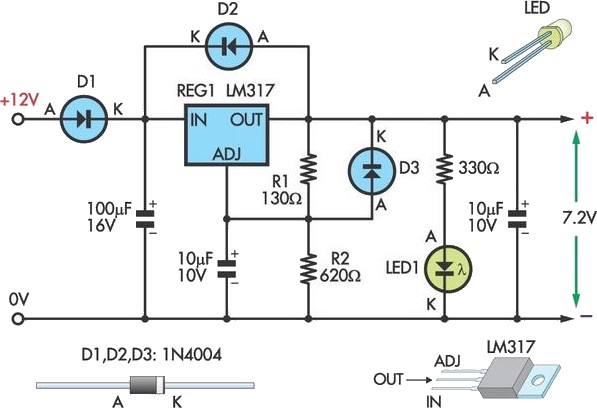
This circuit allows an external 12V SLA battery to power a camcorder that typically operates with a built-in 7.2V battery. Replacement batteries for older camcorder models can be challenging or costly to find. Essentially, the circuit utilizes a standard...
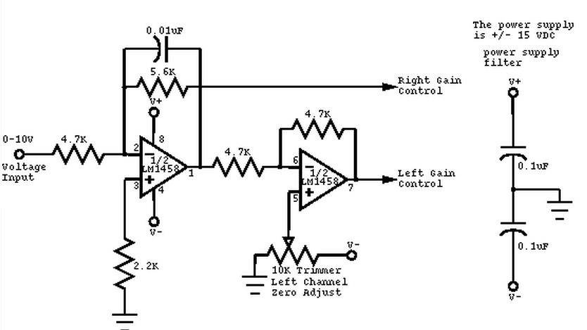
This circuit converts a mono audio signal into a stereo signal that can be panned between the left and right channels using a 0-10V control signal. It is designed for analog synthesizer systems. The circuit operates by taking a single...

This design circuit is for a temperature sensor that utilizes an LM335 integrated circuit (IC) to convert ambient temperature into an equivalent output voltage. The output voltage of the LM335 increases by approximately 10 mV for every 1 degree...

This circuit consists of components Q1, Q2, R1, and C1, which together create a multivibrator. The oscillation produced results in a square wave with a voltage peak-to-peak (Vpp) ranging from 20 to 30 volts. This output is then amplified...
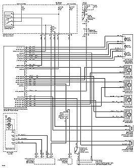
The following circuit illustrates the electrical wiring diagram for the 1997 Chevrolet Malibu. It includes performance circuits for the 2.4L (VIN T) engine and various components. The electrical wiring diagram for the 1997 Chevrolet Malibu is a crucial resource for...
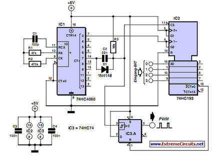
PWM waveforms are frequently utilized to regulate the speed of DC motors. The duty cycle of the digital waveform can be defined using an adjustable parameter. PWM (Pulse Width Modulation) is a technique employed to control the power delivered to...