
Using an inverter transistor monostable circuit diagram
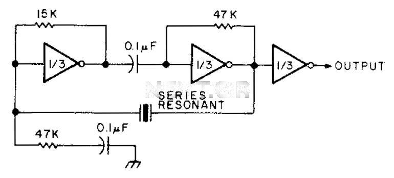
The circuit employs a series resonant crystal oscillator configuration, which is known for its ability to generate stable frequency signals. The inclusion of the triple CD4049 inverter facilitates signal shaping and amplification, allowing for improved performance in RF applications. The CD4049 is a hex inverting buffer, and in this configuration, three of its inverters are utilized to create a robust oscillator circuit.
The resonant crystal is pivotal in determining the operating frequency of the oscillator. It is connected in series with the inverter and other passive components, such as resistors and capacitors, which are essential for tuning the circuit and stabilizing the output frequency. The supply voltage range of 3 to 15 volts provides flexibility in power supply options, accommodating both low-power and higher-power applications.
The low-power characteristics of this circuit make it particularly advantageous for battery-operated devices, extending the operational life of the battery. Additionally, the compact nature of the design allows for easy integration into various electronic projects, including RF transmitters and receivers, where space and power efficiency are critical.
Overall, this circuit design exemplifies an effective approach to creating a portable RF oscillator with minimal power requirements, suitable for a wide range of electronic applications. Circuit diagram all three parts of the series resonant crystal and triple CD4049 inverter connection. Supply voltage range is 3-15V. Compact, low-power RF oscillator portable b attery consumption is very low.
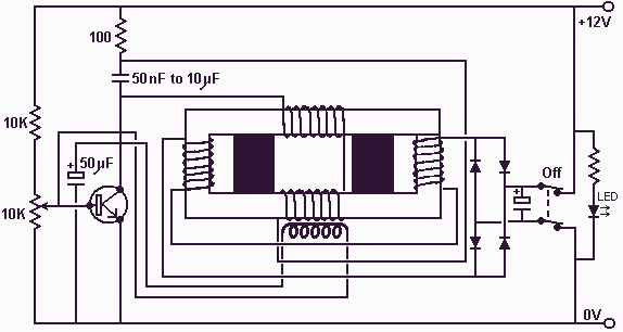
Related Circuits
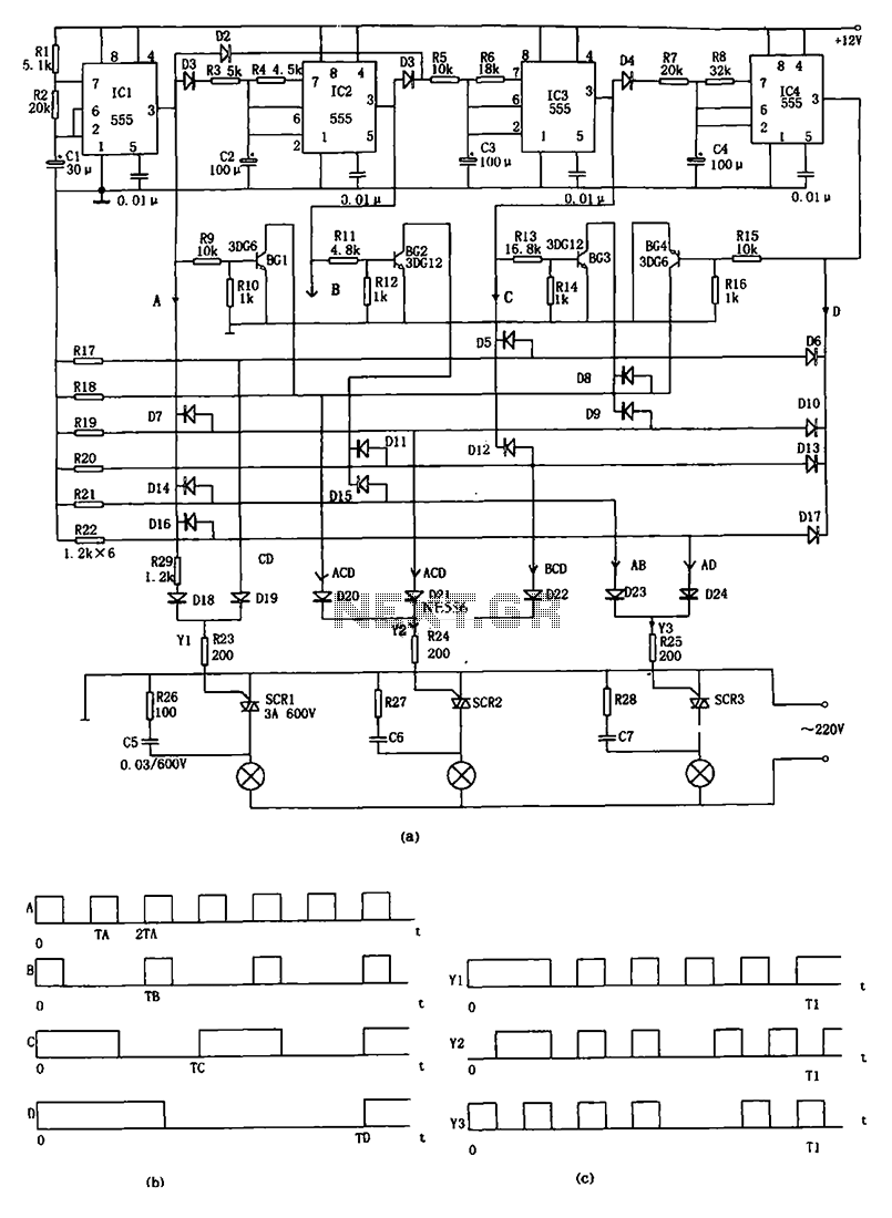
The decorative lamp control circuit is illustrated in the figure. The controller comprises a pulse generator, a frequency divider, a matrix circuit, and a thyristor control circuit. Components IC1, R1, R2, C1, and others form a multivibrator where the...
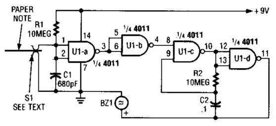
This device prevents paper notes and memos from being overlooked. A paper note placed between two fingers made of a conducting material (metal or conductive plastic) breaks the circuit, allowing pair 1 of Ul-a to go high. The goal...
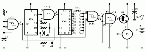
3V battery-powered circuit that emits a beep after a fixed delay of several minutes. This circuit was created in response to requests from users seeking a timer functionality. The described circuit operates on a 3V power supply, making it suitable...

This circuit was designed to obtain a valve-like distorted sound from an electric guitar or other musical instrument. For this purpose a very high gain, three-FET amplifier circuit, was used. The output square wave shows marked rounded corners, typical...

This is a design circuit for a low-cost FM antenna booster that can be used to listen to programs from distant FM stations clearly. The antenna FM booster circuit comprises a common-emitter tuned RF preamplifier wired around the VHF/UHF...
This simple circuit is started running by connecting a twelve volt battery across the terminals, causing the large diameter Light-Emitting Diode to light up. When the battery is removed, the LED stays lit up because the circuit has become...