
Homemade whole integrated circuit amplifiers 01

The circuit design integrates several key features that enhance audio performance and user control over sound characteristics. The operational amplifier serves as a crucial component in the pre-amplification stage, ensuring that the audio signal maintains clarity and integrity despite the inherent losses from tone adjustments. The configuration of the op-amps allows for flexible channel management, enabling independent bass and treble adjustments through the designated components.
The bass adjustment circuit, utilizing resistors such as RP4, provides users with the ability to manipulate low-frequency response, enhancing the depth and richness of audio output. Similarly, the treble adjustment circuit, composed of RP2 and RP3, allows for fine-tuning of high-frequency sounds, ensuring a balanced audio experience across different genres of music.
The volume control mechanism, facilitated by RP5 and RP6, not only manages the loudness but also incorporates a loudness contour feature, which can boost bass frequencies at lower volume settings, catering to listeners who prefer a fuller sound even at reduced levels. The inclusion of output balance controls (RP7 and RP8) further enhances the user experience by allowing for precise adjustments to the stereo soundstage, ensuring that both left and right channels are perfectly matched to the listener's preference.
The power amplification stage, utilizing the TDA2030 IC, is designed for efficiency and compactness. Its ability to deliver substantial output power while maintaining low distortion levels makes it suitable for a variety of audio applications. The V-shaped package design not only minimizes space requirements but also facilitates heat dissipation, which is critical for maintaining performance during extended use.
Overall, this circuit exemplifies a well-thought-out design that combines functionality with user-friendly features, making it an effective solution for enhancing audio playback in various settings. Circuit shown in Figure 5-60 in Figure 6 by the operational amplifier IC op amp set up a channel pre-amplifier to compensate for the loss of tone control circuit caused by inse rtion. Another group of op amp one channel driven stage amplifier circuit to obtain sufficient excitation voltage port RP11. RP4 and other components of the two-channel bass adjustment circuit; RP2, RP3 and other components group into treble adjustment circuits for both channels.
Two-channel volume control circuit is a loudness control circuit t by the RP5.RP6 metadata such pieces of composition. When the smaller volume, bass can be improved accordingly. RP7 RP8 can adjust the output balance of the left and right channel volume. Power amp circuit TDA2030 IC, its shape is V-shaped five-pin single in-line plastic package, the volume is small.
When using when 18V power supply, the load can be obtained not less than 8,0 isw output power armor distortion less than 0.5%. As shown in Figure 5-61 are l. M324 and Tf) A2030 appearance.
Related Circuits
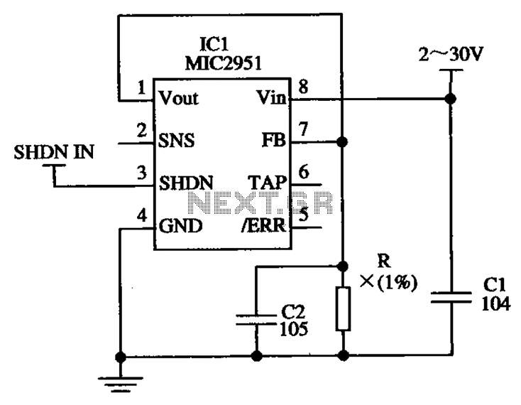
The circuit illustrated in the figure utilizes the low-drift current source circuit MIC2951, which is designed to provide specific output current values. The MIC2951 is a precision voltage regulator that can also be configured to function as a low-drift current...
This is a simple circuit that features high-performance power amplifiers. The power amplifier is available as a PCB, along with a complete list of components. The described circuit utilizes high-performance power amplifiers, which are essential for applications requiring significant signal...
The basic connection circuit for the ISO122/124 includes power and signal connections. Each supply terminal of the ISO122/124 must be equipped with a 1 µF tantalum capacitor serving as a bypass filter. It is important to position the printed...
This universal power supply includes a bridge rectifier, a voltage stabilizer (78xx), and a PNP power transistor. This combination allows for a load current output. The universal power supply circuit is designed to convert alternating current (AC) from the mains...
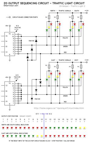
The current application involves the use of the VHDL hardware description language for designing a traffic light system controller circuit. This design is implemented within the Altera MAX PLUS EDA software environment, which facilitates compilation, simulation, and programming for...

Activated this and inadvertently destroyed several 2N3055 transistors by shorting the emitters to ground. In all cases, the transistors opened up, and no damage to the emitter occurred in any transistor. The alternative circuit in Figure 2 will provide...