
Precision tandem type power supply circuit diagram
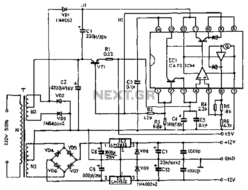
Main Specifications: Input voltage: 220V, 50Hz, with an allowable variation of ±10%; DC output voltage and load current: +5V at 2A, +12V at 1A, and -12V at 1A; output ripple: 30mV; output voltage adjustment range: ±0.5V; includes overload and short circuit protection devices; transformer T parameters: power rating of 35VA, with secondary windings N2 at 2x12V and N3 at 2x15V; operational ambient temperature range: -10 to +40 degrees Celsius.
The circuit operates as a regulated power supply, utilizing a center-tapped transformer to facilitate dual polarity outputs. The transformer generates multiple secondary voltages, which are rectified and filtered to provide stable DC outputs. The CA723 voltage regulator is crucial for ensuring that the output voltages remain within specified limits despite variations in input voltage or load conditions.
The circuit's design incorporates feedback mechanisms that dynamically adjust the voltage output based on real-time measurements, promoting stability and reliability. The use of diodes VD1, VD2, and VD3 ensures that the current flows in the desired direction, while the capacitors smooth out voltage fluctuations, reducing ripple and enhancing the quality of the DC output.
The inclusion of resistors R4, R5, and R6 allows for fine-tuning of the reference voltage, ensuring accurate voltage regulation. The operational amplifier within the CA723 compares the output voltage against the reference, and the feedback loop involving VT1 enables rapid response to changes in load or input conditions, maintaining the desired voltage levels.
Protection features such as overload and short circuit safeguards are essential for preventing damage to the circuit components, ensuring longevity and reliability in operation. The specified temperature range indicates the circuit's suitability for various environments, making it versatile for different applications. Overall, this circuit exemplifies effective design principles in power supply regulation, combining functionality with safety measures for robust performance. Circuit shown in Figure secondary N3 center tap and transformer T common point diode VD2, VD3 positive and capacitance C2, C6, C7 and negative electrode capacitance C9, C10 and other components connected to the positive electrode and the ground, which ground zero. + 5V power supply using a manifold excellent performance of CA723, as an automatic adjustment of the output voltage. By a rectifier diode VD1, filter capacitor C1, a positive DC voltage U1 acquired 11 feet to the CA723, CA723 of 6 feet at a constant voltage, the resistors R4, R5 and R6 partial pressure, the 5 foot can get to a reference voltage.
If the + 5V output terminal voltage increases, the potential of 4 feet elevated CA723, CA723 after the comparator compares the comparison signal is fed to the error amplifier output pin 10 to adjust the low potential tube VT1 base, make VT1 between the collector and emitter voltage increases, the output voltage decreases, to achieve automatic voltage regulator. If the output voltage is reduced, the entire change process will vary in the opposite direction. Main Specifications: Input voltage: 220V, 50Hz, allowable voltage variation of plus or minus 10%; DC output voltage and load current: + 5V 2A, + 12V 1A, -12V 1A; Output ripple 30mA; Output Voltage adjustment range: positive negative 0.5V; the power supply overload and short circuit protection device; transformer T parameters: power: 35VA, N2: 2x12V, N3: 2x15V; ambient temperature: -10 to +40 degrees Celsius.
Related Circuits
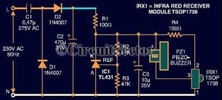
This document presents an infrared remote control tester circuit that can be constructed at a low cost. The circuit is built around the infrared receiver module TSOP1738. The state of the remote control can be observed through the sound...
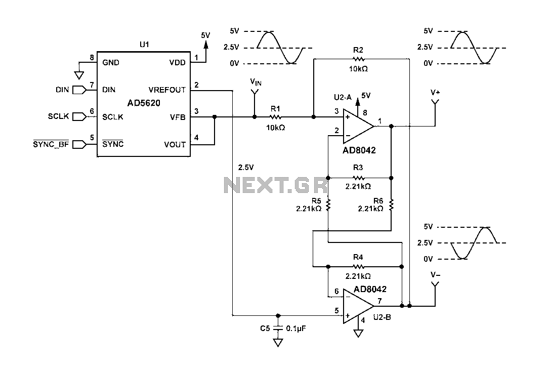
Figure 1 illustrates a circuit that utilizes a single +V power supply and a voltage output Digital-to-Analog Converter (DAC) known as the AD5620. The DAC is controlled via an SPI port, with its output ranging from 0 V to...
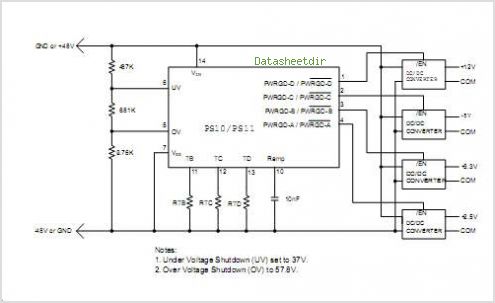
The PS10 saves board space, improves accuracy, eliminates optocouplers or level shifts, and reduces overall component count by combining four programmable timers, input under-voltage (UV) and over-voltage (OV) supervisors, a programmable power-on reset (POR), and four 90V open drain...
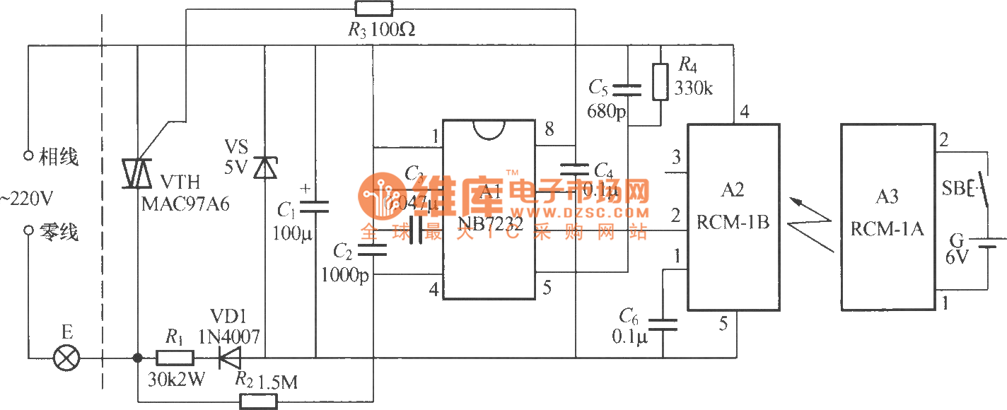
The diagram above illustrates a radio remote control dimmer circuit. This circuit utilizes a micro radio transmit/receive module in conjunction with a light modulation ASIC, resulting in a compact and easily producible design. It operates reliably and features a...

User Agreement & Disclaimer Disclaimer: All files are found using legitimate search engine techniques. This site does not condone hacking into sites to create the links it lists. It is assumed that all links found on the search...
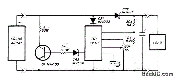
A voltage regulator is connected across the solar cell to prevent damage to the storage battery due to overcharging. A series diode prevents the array from discharging the battery during hours of darkness. The regulator does not draw power...
Warning: include(partials/cookie-banner.php): Failed to open stream: Permission denied in /var/www/html/nextgr/view-circuit.php on line 713
Warning: include(): Failed opening 'partials/cookie-banner.php' for inclusion (include_path='.:/usr/share/php') in /var/www/html/nextgr/view-circuit.php on line 713