
For differential drive circuit diagram of a voltage output DAC AD5620
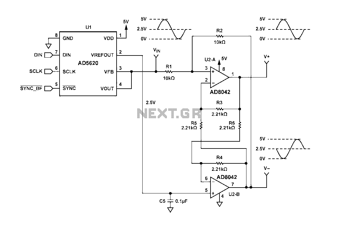
The circuit configuration in Figure 1 is designed to convert digital signals into analog voltages with precision and stability. The use of the AD5620 DAC allows for a high-resolution output, which is essential for applications requiring accurate signal representation. The control of the DAC through an SPI interface facilitates straightforward integration with microcontrollers or digital signal processors, enabling efficient data transfer and command execution.
The reference voltage of +2.5 V plays a critical role in maintaining the accuracy of the output signal. With a temperature coefficient of 5 ppm/°C, the reference voltage source ensures minimal drift over temperature variations, which is vital for applications in environments with fluctuating temperatures. The common-mode voltage of +2.5 V at the V-side output allows for optimal operation of the AD8042 differential driver, which is designed to amplify the differential signal while rejecting common-mode noise.
The feedback network associated with U2-B is crucial in determining the gain and phase characteristics of the circuit. By forcing a 180-degree phase shift at the V+ terminal, the circuit can effectively manage the output characteristics, ensuring that the signal integrity is preserved. This phase manipulation is particularly important in differential signaling applications, where maintaining the correct timing and phase relationships between signals is critical for performance.
Overall, the circuit depicted in Figure 1 represents a robust solution for generating precise analog outputs from digital inputs, suitable for a wide range of electronic applications. The careful selection of components and configuration ensures high performance and reliability in signal processing tasks.Figure 1 circuit uses a single +V power supply, and a voltage output DAC AD5620. DAC input by an SPI port control. DAC output swing from V to +5 V. Within the DAC chip referenc e voltage source (+2.5 V) to set the AD8042 differential driver circuit common-mode voltage. The temperature coefficient of the reference voltage source is 5 ppm/C. V -Side output common-mode voltage of +2.V is centered inverted DAC output. U2-B feedback network and forcing V + terminal voltage V Terminal voltage phase by 180. Figure 1. Voltage Output DAC AD5620 differential driver
Related Circuits
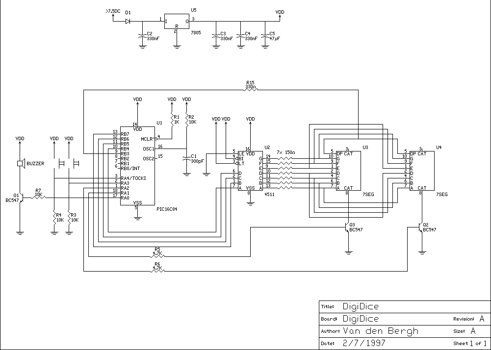
This is a digital dice circuit that uses the PIC16C84. The digital dice circuit utilizing the PIC16C84 microcontroller is designed to simulate the random rolling of a standard six-sided die. The circuit operates by generating a random number between 1...
A newcomer to electronics has questions regarding the interpretation of circuit diagrams. There is uncertainty about the arrangement of wires in these diagrams. Understanding circuit diagrams is essential for anyone involved in electronics, as they serve as a visual representation...

Sometimes it is necessary to power a circuit from a battery where the required supply voltage falls within the discharge curve of the battery. If the battery... Powering a circuit from a battery involves understanding the discharge characteristics of the...
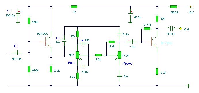
The first BC109C transistor (on the left side) functions as a buffer, offering the circuit a high input impedance of approximately 250k ohms and a voltage gain slightly less than unity. As the Baxandall tone control circuit is a...
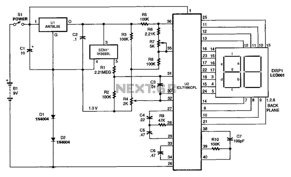
The output DC voltage of sensor SEN1 changes linearly in response to variations in relative humidity. This DC voltage is routed through resistors R1 and R2 to the analog-to-digital (A/D) converter chip U2. Resistor R4 is connected to ground,...

The circuit utilizes a dual operational amplifier integrated circuit (IC), specifically the 1458, which contains two separate op-amps within a single package. In this configuration, the first op-amp functions as a voltage follower, directing its output to charge capacitor...