
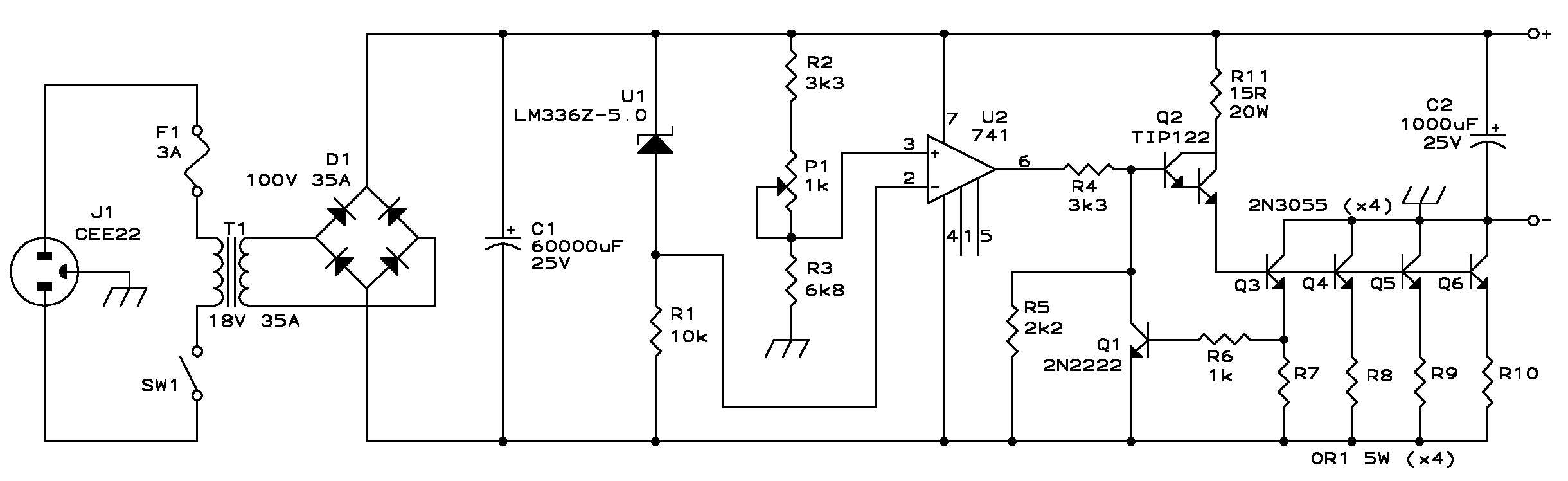
0-15 Volt 0-1A Power supply

The described circuit operates as a constant current source for a bank of three zener diodes, ensuring stable voltage output despite fluctuations in the supply voltage. A critical component, TR1, regulates the current flowing through the zener diodes, while the resistor Rx serves as a current sensing element. In the event of excessive current, Rx activates a protective mechanism to disconnect the zener diodes, thereby safeguarding the circuit.
The logarithmic taper potentiometer (1M0) enables fine-tuning of the current threshold via TR2, allowing for an adjustable response to varying load conditions. The calculation for Rx is based on the formula (0.7/Amperes) ohms, where the maximum output of the power supply unit (PSU) dictates the value of Rx. In this prototype, with a maximum output of 1 ampere, Rx is set to 0.5 ohms, with a power rating of at least 1 watt to prevent overheating.
The zener diodes provide a stable reference voltage of 10.7 volts with intermediate tappings at 4.7 volts and 7.7 volts. The 7.7-volt tapping serves as the reference point for a 6-volt swing, which is adjustable using a 50K potentiometer. This swing is subsequently amplified by an operational amplifier configuration consisting of transistors TR3, TR4, TR5, and TR6, achieving a voltage gain that extends the output range to 0 to 15.4 volts.
The full-wave rectifier, utilizing 1N5401 diodes rated for 3 amperes, converts the 15-0-15 volt AC input from the transformer to a stable DC output. The design considers the charging characteristics of the large 2700uF capacitor, which may require higher-rated diodes if increased capacitance is employed. The prototype also includes two parallel 47000uF capacitors to enhance output current capability.
Thermal management is crucial, particularly for the TIP31 output transistor (TR6), which requires a heatsink due to significant power dissipation. With an output voltage as low as 0.1 volts and a pre-regulator voltage of 18.1 volts, the TIP31 can dissipate up to 18 watts. Adequate heatsinking is essential, with a calculated minimum surface area of 100 square cm to maintain safe operating temperatures.
For applications requiring higher current outputs, the circuit can be modified by replacing TR6 with a darlington pair configuration, such as TIP31 combined with 2N3055, while ensuring that other components like the rectifier and reservoir capacitor are appropriately rated for the increased load. The heatsink design incorporates three aluminum sheets, allowing for effective thermal dissipation through a substantial surface area, further enhancing the reliability of the power supply unit.TR1 provides a constant current to a bank of three zener diodes, thus maintaining a constant voltage independant of supply voltage variations. The resistor Rx is used to sense the PSU output current and to switches off the current to the zener diodes should the output current become excessive.
The 1M0 (logarithmic taper) pot causes the current sensor (TR2) to "kick-in early", so providing a variable current threshold limit. The value of RX should be (0.7/Amperes) ohms, where Amperes is the maximum output of the bench PSU. The prototype was set to 1-ampere, so Rx should be 0.5 / 1.000 = 0.5 ohms. The resistor should be rated at 1-watt, or 2x 1R0 500mW resistors in parallel for 1-ampere maximum output.
I have used 4x 1R0 ohms in parallel (0.25 ohms) and have achieved 2-amperes (with a bigger heatsink). The reference diodes provide a voltage reference of 10.7-volts with tappings at 4.7-volts and 7.7-volts. The 7.7-volt tapping is used as the reference voltage. In this way we have a 6-volt swing selected by the 50K voltage pot, above and below the 7.7-volt reference.
This voltage swing is amplified by the operational amplifer formed by TR3, TR4, TR5 and TR6. The DC output of the Op-Amp is arranged to give a voltage gain of a little over 2, so the 4.7-volts to 10.7-volts reference will become 0 to 15.4-volts at the output. I had thought about using PCB mounting pots, but the finished PCB is quite large and the heatsink must be quite substantial (see below).
Here is the finished PSU PCB. I must emphasise that this is a prototype and not the final PCB which is much better in the layout. A full-wave rectifier provides the 18-volts input from a 15-0-15 volt mains input transformer. The diodes 1N5401 are rated at 3-amperes. At first sight, it would appear that 1-Ampere diodes, such as 1N4001, would suffice, but this is not the case. Althought the averge current through these diodes is alittle over 500mA, the 2700uf input capacitor will be charged with short pulses, each considerably higher than 500mA.
If the 2700uf capacitor were to be increased in value, then the rectifier diodes may need to be rated even higher. I used two parallel 47000uf in the prototype PSU, mainly because I wanted more output current so an additional regulator transistor is to be added.
By the way, the supply smooting capacitors are not mounted on the board.Note that the TIP31 output transistor MUST be fitted with a heatsink.With minimum output voltage (say, 0.1vDC) and an 18.1v pre-regulator voltage, the TR6 TIP31 output transistor will be dissipating 18v x 1A = 18 watts. If we allow the device temperature to rise TO 120°C then we can allow an increase of 90°C over the ambient room temperature.
90°C / 18watts = 5°C per watt. A heatsink of 100 square cm is therefore required. If you wish to pull more current from this PSU then you will need a larger heatsink and change the value of Rx accordingly. Up to about 3-amperes is quite possible. TR6 may also be replaced with a darlington pair power transistor (such as TIP31 + 2N3055) if you want more than 3-Amperes, more attention will be required to other parts of the circuitry, such as the rectifier and reservoir capacitor.
The heatsink shown above is three pieces of thin aluminium sheet, 11cm x 3cm drilled with a 3mm hole dead centre. These are bolted between the PCB and the TIP31 transistor before any other components are mounted on the board.
The fins can now be bent up to form six fins, each 5cm x 3cm or a total surface area of 180cm square. This is a little bigger than the calculation, but to over-engineer is not a fault (at least, not in my opinion).
Here is the completed project. 🔗 External reference
Related Circuits
Build a 20 Amp 13.8 Volt Power Supply. There are some electronic applications where it may be necessary to run relatively high current circuits, such as transformers. To construct a 20 Amp, 13.8 Volt power supply, the following components and...
This is a positive high-voltage hot swap controller circuit with a power limiter. This circuit utilizes the TPS2491 or TPS2490, as both of them have specific features. The positive high-voltage hot swap controller circuit is designed to safely connect and...

Common mode input voltage up to a difference of 100V enlarged circuit diagram. The circuit diagram described features a design capable of handling a common mode input voltage with a differential range of up to 100V. Such a configuration is...
This project represents an older design that has likely been replaced by a newer version. Nevertheless, it remains a functional design and can be beneficial for homebrew synthesizer enthusiasts. It should be noted that the majority of these designs...
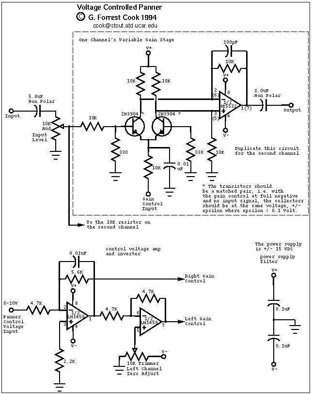
This circuit is used to convert a mono audio signal into a stereo signal that can be panned between the left and right channel by a 0-10V control signal, it is intended for analog synthesizer systems. The circuit is...
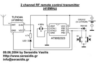
The following circuit illustrates a 3V power supply designed for an RF remote control circuit. This circuit is based on the AT90S2323 integrated circuit (IC). Features include a data rate of 2400 bps. The 3V power supply circuit for the...