
1.2GHz VCO With Linear Modulation circuit using MAX2754
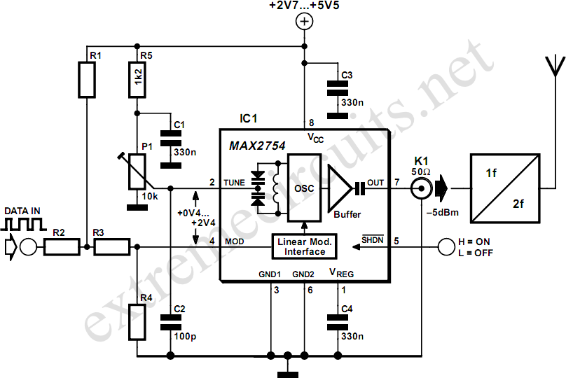
The MAX2754 integrated circuit is designed to operate as a high-frequency VCO, providing a reliable solution for applications requiring precise frequency generation and modulation. The ability to adjust the center frequency using the TUNE input allows for flexibility in various RF applications, especially in communication systems where tuning to specific frequencies is essential. The modulation capabilities via the MOD input enable the device to accommodate both digital and analog signals, making it suitable for applications such as frequency shift keying (FSK), which is commonly used in digital communication systems.
The resistors R1 to R4 play a crucial role in shaping the data signal to meet the modulation requirements. By adjusting these resistors, the user can set the amplitude and offset of the input signal, ensuring that the VCO responds appropriately to the modulation input. The specified resistor values for a 5 V supply provide a practical example of how to configure the circuit for optimal performance.
The output stage of the MAX2754 is designed to deliver a robust signal level, suitable for driving a 50 Ω load. The internal coupling capacitor simplifies the design by eliminating the need for external components, thereby reducing the overall footprint of the circuit. This feature is particularly advantageous in compact RF designs where space is limited.
For applications operating in the 2.4 GHz ISM band, the incorporation of a frequency doubler is necessary to achieve the desired output frequency. The circuit diagram illustrates this configuration, emphasizing the relationship between the MAX2754, the frequency doubler, and the 2.4 GHz antenna. This integration facilitates seamless transmission in the ISM band, catering to a wide range of industrial, scientific, and medical applications. Overall, the MAX2754 provides a comprehensive solution for high-frequency oscillation and modulation, streamlining the design process for RF engineers.Since high frequency voltage-controlled oscillators, or VCOs, are not easy to construct, Maxim ( has produced an integrated 1. 2GHz oscillator, the MAX2754. The center frequency is set using the TUNE input, and a linear modulation input allows the frequency to be modulated.
The IC is available in an 8-pin µMAX package, operates from a supply of be tween 2. 7 V and 5. 5 V, and draws a current of less than 2 mA. Both TUNE and MOD operate over control voltage range of +0. 4 V to +2. 4 V. TUNE allows the VCO frequency to be adjusted from 1050 MHz to 1270 MHz. In some applications a PLL control voltage will be applied here, allowing the center frequency to be set exactly to a desired value. For simplicity in the circuit diagram we have shown a potentiometer. The MOD input allows the VCO to be modulated in a digital or analogue fashion, with a transfer slope of 500 kHz/V.
In the circuit we have shown an example where MOD is used for frequency shift keying (FSK) modulation. Resistors R1 to R4 shift the level of the data signal so that it has a center value of +1. 4 V and an amplitude corresponding to the desired frequency deviation. One example set of values, suitable for use with a 5 V power supply, is as follows: R1 = 480 , R2 = 100 , R3 = 220 und R4 = 270 .
The input impedance is about 1 k. The output level of the MAX2754 at OUT is around 5dBm into 50 . A coupling capacitor is not required here: the IC already contains one. The MAX2754 is designed for use in transmitters in the 2. 4GHz ISM (industrial, scientific and medical) band. This requires the addition of a frequency doubler, which, along with the 2. 4GHz antenna, is shown symbolically in the circuit diagram. 🔗 External reference
Related Circuits
The circuit is a battery charging system powered by Q2, Q6, R8, and D10, which provides constant current to charge the battery. When an external power supply is present, the charging current flows through R8 and D10 to charge...
PWM waveforms are frequently utilized to regulate the speed of DC motors. The duty cycle of the digital waveform can be defined using an adjustable parameter. PWM (Pulse Width Modulation) is a technique employed to control the power delivered to...
The following circuit illustrates a super fast Ni-Cd battery charger. It is based on the IC MAX 712 and is designed to charge a Ni-Cd battery at a rate of 300 mA. The circuit utilizes the MAX 712 integrated circuit,...
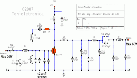
This circuit functions as an RF power amplifier designed to operate with a power supply capable of delivering 13 volts at a current of 10 amperes. Careful assembly of the power source is essential. It utilizes a shielded transformer...
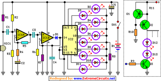
The basic circuit illuminates up to ten LEDs in sequence, following the rhythm of music or speech picked up by a small microphone. The expanded version can drive up to ten strips, each formed by up to five LEDs,...
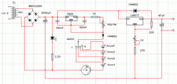
This circuit consists of two main components: a battery charger that provides a fixed output voltage of 5V DC, and a regulated power supply that allows for an adjustable output voltage ranging from 2 to 9 volts. The circuit design...
Warning: include(partials/cookie-banner.php): Failed to open stream: Permission denied in /var/www/html/nextgr/view-circuit.php on line 713
Warning: include(): Failed opening 'partials/cookie-banner.php' for inclusion (include_path='.:/usr/share/php') in /var/www/html/nextgr/view-circuit.php on line 713