
1 mA CURRENT SINKl
25/R 2. In actual use, the R2 always uses the 1W resistance. When the R2 is 25 ©/1W, the charging current of the battery is about 50mA. The charging indicator circuit is composed of the resistor R1 and LED, if we choose the appropriate value of R3, when the battery has the required charging voltage, the VT1 will cut off, the LED will turn off. This circuit can charge more than four No. 5 nickel-cadmium batteries. (View) The adjustable power charger circuit which is introduced in this article has the highest charge voltage of 12V, the maximum charging current is 200mA.
The adjustable voltage range is 0-12V, the adjustable current range is 0-200mA, and it has the constant voltage, trickle charging mode. The circuit is as shown in figure 3-2. When the battery voltage rises to the set value, the circuit will stop operating. You can change the charging voltage by adjust the duty ratio of R2. When the voltage of the battery is full, the voltage-regulator diode VD6 punctures the conduction to trigger the conduction of the transistor VT, the green indicator light LED2 turns on, and the pin-4 of time-base circuit has the low level to stop the oscillation of the circuit, the pin-3 has no output voltage.
(View) The voltage stabilization sampling and error amplification system is composed of the pin-1 and pin-2, the positive phase input port pin-1 inputs the 15V DC voltage which is rectified and output by the inverter sub-sampling winding, and this 15V DC voltage is divided by R1 and R2 to supply the 4. 7 ½ 5. 6V sampling voltage to the inverter. The reverse phase input port pin-2 inputs the 5V reference voltage which is output by the pin-14. When the output voltage decreases, the voltage of pin-1 decreases too, the error amplifier outputs the low level to rise the output voltage through the PWM circuit.
The voltage of pin-1 is 5. 4V, the voltage of pin-2 is 5. 0V, the voltage of pin-3 is 0. 06V. At this time the output AC voltage is 235V (square wave voltage). (View) The circuit is as shown in figure 3-3. When the battery or storage battery which has lacking voltage is connected between A and B, the partial voltage value of the RP1`s sliding port can not conduct VT5, the VT4 conducts, the resistance R9 is in the positive bias condition to conduct VT3, VT2, VT1, the VT6 turns on, the circuit is in the charging state. You can change the charging current by adjusting RP2`s sliding port. As the voltage of the battery or the storage battery is gradually increased, the partial voltage value of the RP1`s sliding port conducts VT5, the VT4, VT3, VT2, VT1 conduct, the VD6 turns off to indicate the end of charging.
VT1 sets three emitter resistances with different resistance values through S2. (View) This device uses the 220V power grid as hte power supply. The output voltage is adjusted to the set value by potentiometer R1. The main technical data: Operating voltage:-23+/-15%V;Output voltage:-(14-15)V;Output voltage changing rate (when the operating voltage changing rate is +/-15%):<+/-0. 5%;Output resistance (I=4. 5A):<0. 05 ©;Maximum output current:5A;Transistor T3 radiator thermal resistance:<100K/W;Each power transistor radiator thermal resistance:<5. 5K/W. (View) This integrated AVR has three adjustable ports with the lowest base voltage of 1. 25 V which have perfect performance on keeping a steady output voltage. Besides, adjustable port has a super small current which is only about 50 A and super steady with a difference of 0.
5 A. Therefore, it can be used to form constant current and high frequency circuit. Its output current is Id plu 🔗 External reference
Related Circuits
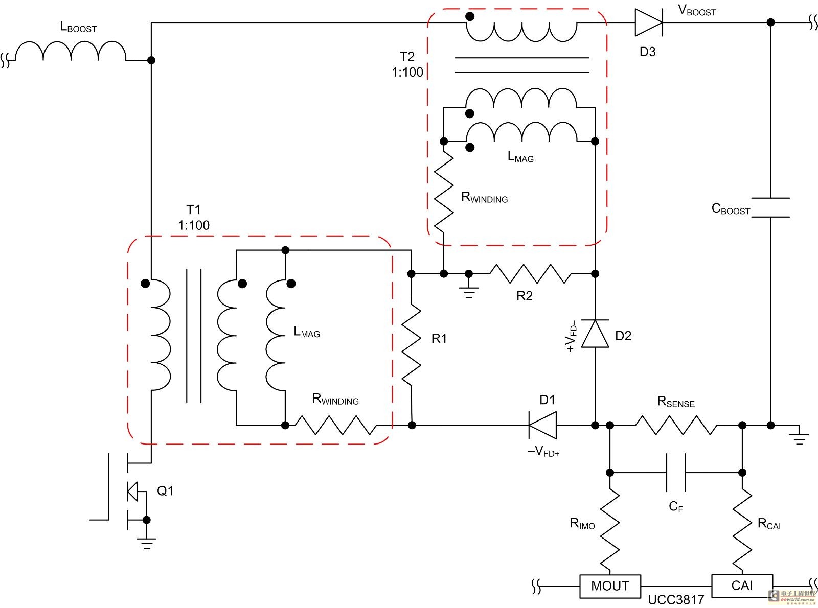
Mode control of the average current (CMC) is necessary to regulate the overall waveform of electric current during the rebuilding cycle. This text recommends selecting specific parameters related to the voltage transformer and outlines steps for designing a circuit...
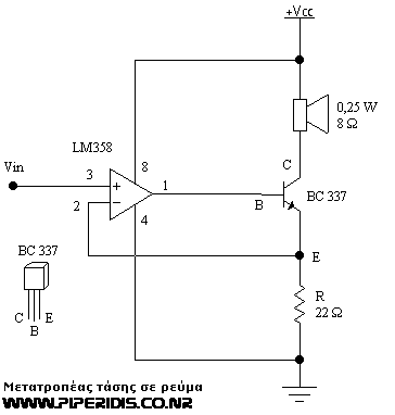
This circuit is one of the simplest voltage-to-current converters designed to drive low loads. In this example, a small 0.25-watt speaker with an 8-ohm resistance is utilized. It is suitable for microcontroller applications or any circuit that employs PWM...
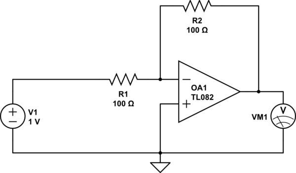
Considering a simple circuit as illustrated below, when the voltage source activates suddenly (changing from 0V to 1V), current will flow through the resistor R1. Assuming an ideal operational amplifier (op-amp) that draws no current, and an ideal voltmeter...
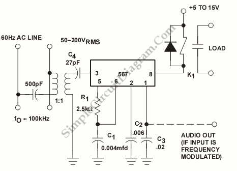
The 567 IC tone decoder/detector can be utilized to construct a remote control or intercom system. This circuit is capable of controlling a relay or transmitting an audio signal. The 567 IC is a versatile component often employed in tone...

A filter removes the DC component of the rectified AC, which is then scaled to RMS. The output is linear from 40 Hz to 10 kHz or higher. The described circuit primarily consists of a filter designed to eliminate the...
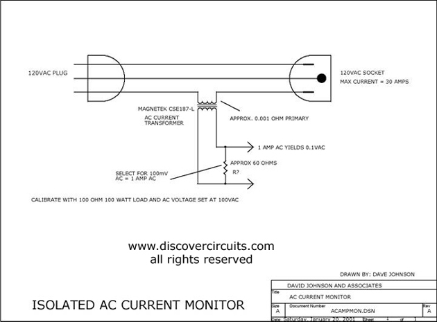
This circuit utilizes a small AC current transformer from Magnetek to generate an isolated voltage that is proportional to the AC current flowing through the primary winding. The AC current transformer operates on the principle of electromagnetic induction, where the...