
10 300V variable power supply circuit design diagram electronic project
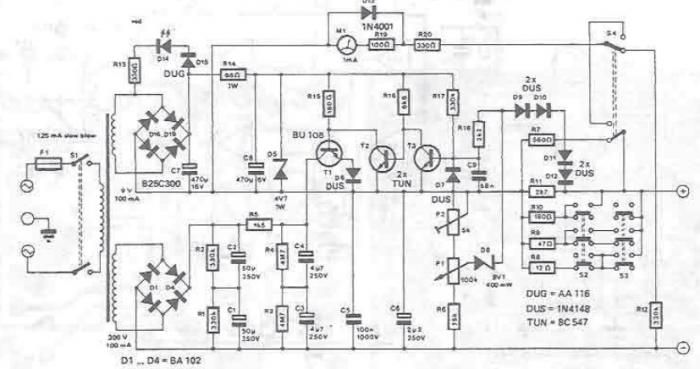
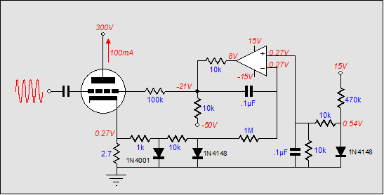
The described DC power supply circuit is designed to deliver a versatile voltage output, adjustable between 10 and 300 volts, making it suitable for various applications. The transformer is a critical component, providing the necessary high voltage and stabilization through its dual windings. The rectification process, facilitated by diodes D1 and D4, converts the AC voltage from the transformer into a higher DC voltage (420 V), which is then filtered to ensure a smooth output.
The use of two electrolytic capacitors rated at 350 V in series is essential for maintaining voltage stability and preventing overvoltage conditions. The parallel resistors (R1 and R2) play a crucial role in balancing the voltage across these capacitors, ensuring that they share the load equally and enhancing the reliability of the power supply.
Resistor R5 is strategically included to reduce power loss in transistor Q1, which is vital for maintaining efficiency within the circuit. The RC network composed of resistors R3 and R4 and capacitors C3 and C4 further stabilizes the input voltage to the collector of Q1, ensuring that it operates within safe limits while providing the required output voltage.
Transistors T2 and T3, specified as BC547, are chosen for their suitability in low voltage and current applications, thus ensuring that the circuit remains efficient without the need for high-power components. The inclusion of diode D7 serves as a protective measure for transistor Q3, safeguarding it from potential negative voltage spikes that could otherwise damage the transistor.
The ability to set multiple current thresholds through a six-pole switch enhances the circuit's versatility. This feature allows for precise control over the output current, catering to different operational requirements. The design thus provides a comprehensive solution for applications requiring adjustable high voltage DC power, with built-in protections and efficient voltage regulation.Using high voltage transistors can be designed a DC power supply that can provide a supply voltage between 10 and 300 volts which can be adjusted with the potentiometer P1. Transformers typically used in such sources have several windings of high voltage and low voltage winding.
In this case we used a winding high voltage 300 V, while a winding 9 V supply was used for circuit stabilization. This circuit is very simple and need not explain. Redressing the secondary voltage (300 V) with diodes D1. D4 are obtained 420 V. filter it, must be connected in series with two electrolytic capacitors rated voltage of 350 V. Two resistors (R1, R2) connected in parallel ensure equal voltages on the two capacitors. R5 resistance reduces power dissipation of Q1 and, together with a second RC network (R3, R4, C3, C4), feed collector of Q1 with a filtered input voltage of 350 V. The transistors T2 and T3 can be BC547 type, because they have nothing to do with voltage and high current.
Diode D7 protects the base of Q3 against excessive voltage peaks negative. You can set four different thresholds of current through the second switch keyboard with 6 poles: 1 mA (no switch pressed), 5 mA (S2 down), 15 mA (S2 and S3 hold) and 50 mA (only S3 down ). 🔗 External reference
Related Circuits
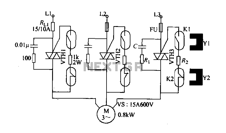
The circuit diagram illustrates a female textile machine power control circuit. VTH1-VTH3 represent TRIACs, while R and C form the absorption line. Rz serves as the triggering current limiting resistor. K1 is designated for starting the reed, and K2...
As circuit power supply voltages decrease and green energy trends gain popularity, designers should re-evaluate circuits that continuously consume power to reduce overall system power consumption. One such circuit is the "normally-ON" circuit, which can now be redesigned with...
A two-battery powered light touch delay circuit designed for convenience at night. It can be placed on a bed pillow, and when the metal contact M under the capsule is touched, a small lamp will automatically light up. The...
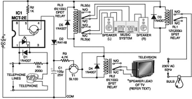
A telephone line-based audio muting and light activation circuit. Frequently, when listening to music or watching television at elevated volume levels, it becomes difficult to hear a telephone ring, resulting in missed important calls. This circuit is designed to address...
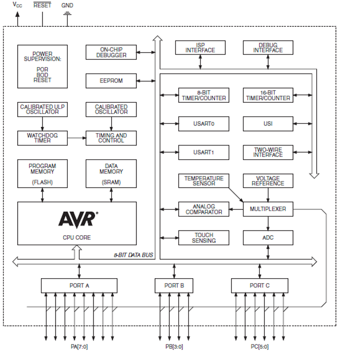
The ATtiny1634 8-Bit AVR Microcontroller from Atmel is based on the enhanced RISC architecture of AVR. It can execute powerful instructions in a single clock cycle, achieving throughputs close to 1 MIPS per MHz. This allows system designers to...
It is embarrassing to acknowledge that the blog post from April 29 contained several schematic errors of my own making, particularly in the variation of Morgan Jones's circuit. One of the resistor values was incorrect by a factor of...