
Digital circuit touch delay circuit 5
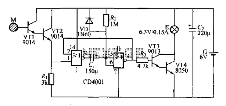
The described circuit is a practical solution for providing temporary lighting in low-light conditions, such as during the night. The use of a touch-sensitive mechanism allows for easy activation without the need for physical switches, enhancing user convenience. The integration of the NOR gate facilitates a simple yet effective timing function, ensuring that the light remains illuminated only for a limited duration, which conserves battery life.
The circuit's design employs two transistors (VT1 and VT2) to amplify the signal generated by the human touch. This amplification is crucial for ensuring that even a minimal touch can trigger the circuit, making it highly sensitive and responsive. The choice of a NOR gate for the logic component is advantageous due to its versatility and availability in standard digital ICs, such as the CD4001. This IC can accommodate multiple NOR gates, allowing for additional functionality or redundancy in the design.
In terms of component selection, the resistor and capacitor values should be chosen based on the desired delay time and the characteristics of the light bulb used. The resistor limits the current flowing through the circuit, while the capacitor determines the timing interval before the circuit resets to its initial state. Careful consideration of these components will ensure reliable operation and longevity of the circuit.
Overall, this light touch delay circuit exemplifies a thoughtful approach to solving common nighttime lighting challenges, combining simplicity, efficiency, and ease of use in its design.A two battery-powered light touch delay circuit, it can be placed on the bed pillow, nighttime convenience, to touch metal M under the capsule on a small lamp will automaticall y light F Zmin around. Indiscriminately, the NOR gate I, or non-f J and peripheral components single -shot timing circuits, or usually J output terminal pin is low level, the three shake tube VT3, VT4 off, small l E does not shine. Night Q. Just touch when needed temporary lighting F electrode sheet M, the human body sensors of clutter signal by VT1, VT2 amplification, the signal is a half weeks so that is input NOR gate L first O pin goes high, pin output low power level, the NOR gate foot jump goes high, the circuit into the temporary steady state, and VT3, VT4 conduction, small lamp E will be powered light.
At this power by R, to C, charging the two input terminals NOR gate of, song lu foot stretch rising after about about 2min, paid back to the steady state of the NOR gate circuit feet of recovery low, small light F off. Or rli, NOR gate may be a quad 2 input NOR gate CD4001 digital integrated circuits, so that the manifold in use when the other two unused input NOR gate terminal, namely, a foot all connected with the negative terminal of the power supply G may not be vacant, in order to eliminate the potential interference ten.
Related Circuits
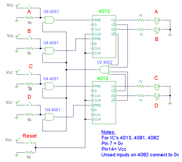
This design utilizes four integrated circuits (ICs) and features four input circuits with four independent outputs, along with a single master reset switch. The outputs are configured with light-emitting diodes (LEDs), which can be modified to control lamps or...
Most universal radio receivers have a very wide bandwidth that is not particularly suitable for radio amateurs. The better models with narrower bandwidth are almost a... Universal radio receivers are designed to operate over a broad frequency range, making them...
FGDF-3 is a three-phase low-temperature iron plating main circuit, while the KGDF-3 represents a low-temperature iron plating power supply device that includes characteristics of a single-phase low-temperature iron plating power supply. This device utilizes a three-phase power grid to...
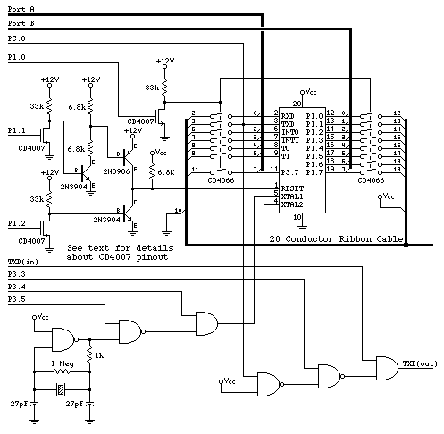
This is a beta release schematic. Use at your own risk. The idea is to add this circuitry to a board that already has RAM at address 2000 and an 82C55 I/O chip to provide ports A, B, and...
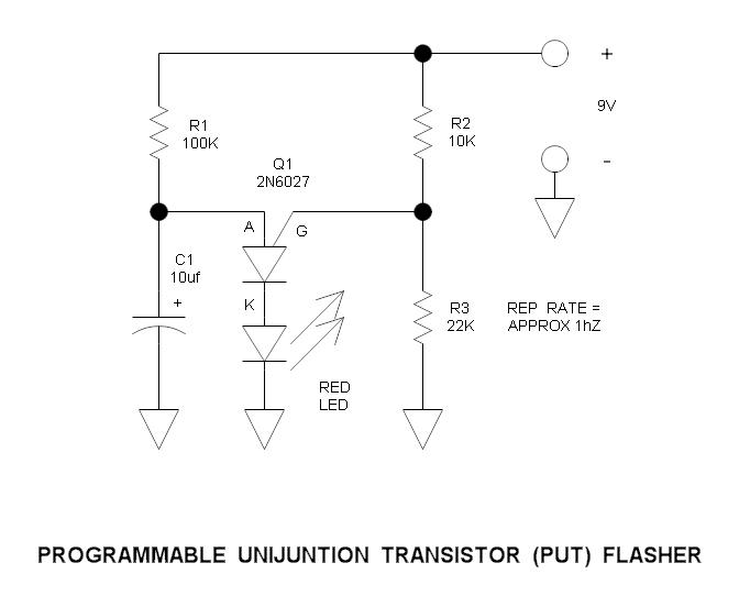
This is a simple circuit that illustrates the function of the programmable unijunction transistor. It can be quickly wired on a proto-board. The circuit utilizes a programmable unijunction transistor (PUT) to demonstrate its operation as an oscillator. The PUT, which...
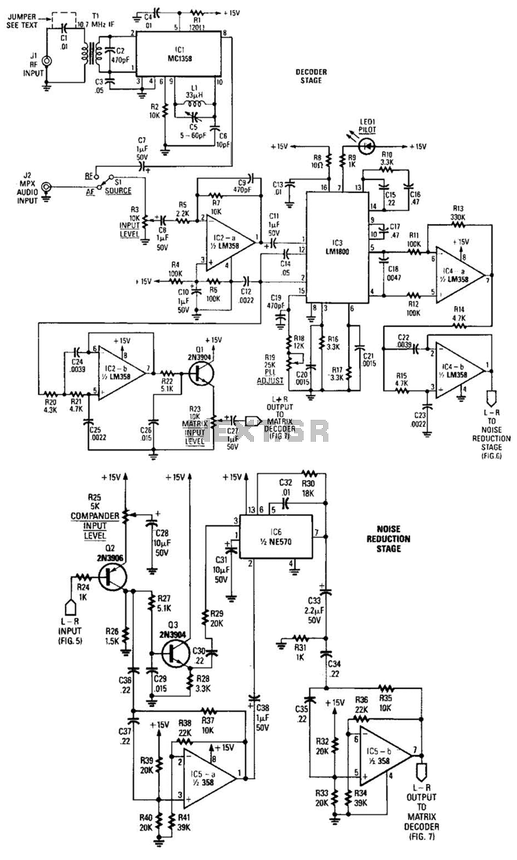
A block diagram of the stereo-TV decoder illustrates the overall relationships between the distinct sections of the circuit, while additional details of each subsection are provided. The decoder section is centered around TCI, a standard 4.5-MHz audio demodulator. The...
Warning: include(partials/cookie-banner.php): Failed to open stream: Permission denied in /var/www/html/nextgr/view-circuit.php on line 713
Warning: include(): Failed opening 'partials/cookie-banner.php' for inclusion (include_path='.:/usr/share/php') in /var/www/html/nextgr/view-circuit.php on line 713