
10 Mhz fiberoptic receiver

The described circuit functions as a high-speed optical signal receiver, suitable for applications requiring precise light input conditioning. The use of a PIN photodiode as the initial light detection component allows for efficient conversion of optical signals into electrical signals. The broadband feedback amplification stage (Q1-Q3) ensures that the signal is amplified effectively across a wide frequency range, maintaining fidelity and minimizing distortion.
Following the initial amplification, the design incorporates a second amplification stage that further increases the signal strength, allowing for robust processing of the optical input. The two-way peak detector (Q6-Q7) is essential for tracking the maximum and minimum levels of the input signal, enabling dynamic range compression and ensuring that the system can adapt to varying signal amplitudes without loss of information.
The junction of the 0.005 µF capacitor and the 22-ohm resistor serves a critical role in stabilizing the DC output signal from Q5. This midpoint voltage is crucial for setting a reference level that is independent of the signal's amplitude, allowing for consistent triggering of subsequent stages in the circuit. The buffering provided by the LT1012 ensures that this reference voltage is stable and low bias, minimizing any potential loading effects on the circuit.
The LT1016 comparator is utilized to process the buffered signal, with its positive input receiving the adaptive voltage and its negative input connected directly to Q5's collector. This configuration allows for accurate comparison and triggering based on the conditioned optical signal, facilitating rapid response times necessary for high-frequency applications. Overall, this circuit design exemplifies effective signal conditioning for high-speed optical communications, ensuring that input signals are accurately processed for further electronic analysis or transmission.The receiver will accurately condition a wide range of light inputs at up to 10 MHz data rates. The optical signal is detected by the PIN photodiode and amplified by a broadband fed-back stage, Q1-Q3. A second, similar, stage gives further amplification. The output of this stage (Q5's collector) biases a 2-way peak detector (Q6-Q7). The maximum peak is stored in Q6's emitter capacitor while the minimum excursion is retained in Q7's emitter capacitor.
The dc value of Q5's output signal's mid-point appears at the junction of the 0.005 µ capacitor and the 22 ohm unit. This point will always sit midway between the signal's excursions, regardless of absolute amplitude. This signal-adaptive voltage is buffered by the low bias LT1012 to set the trigger voltage at the LT1016's positive input.
The LT1016's negative input is biased directiy from Q5's collector.
Related Circuits

By adding one integrated circuit and some passive components, the previously developed 40-meter direct conversion receiver design has been transformed into a superheterodyne model. The advantages of single signal reception in this circuit are particularly appreciated by those who...
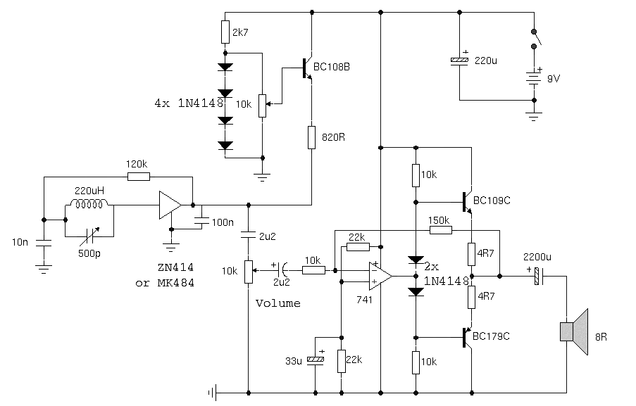
The circuit demonstrates the application of the ZN414 integrated circuit (IC) to create a compact AM radio receiver. The ZN414 IC is a combination of a transistor and a tuned radio frequency (TRF) circuit. The ZN414 IC is specifically designed...
This reflex radio project was inspired by Robert Bazian's design. His reflex radio is the "darndest" thing I have seen and his spectacular results inspired me to come up with my own version! These designs are similar to two-transistor...

XTAL1 drives amplifier Q3/Q4, which is tuned to 2.25 MHz. The detected signal is fed to audio amplifier IC1. A 9-V supply is used. The circuit operates at 2.25 MHz and is designed to be used with an ultrasonic...

This circuit generates audio musical notes that can be heard from a distance of up to 10 meters. The circuit is divided into two parts: an infrared (IR) music transmitter and a receiver. The circuit operates on the principle of...
Burr-Brown DRV134 audio balanced line receiver schematic PCB/kit available? There is an interest in creating a balanced line receiver using the DRV134. The Burr-Brown DRV134 is an integrated circuit designed for audio applications, specifically for converting unbalanced audio signals...