
10-W Class A Amplifier
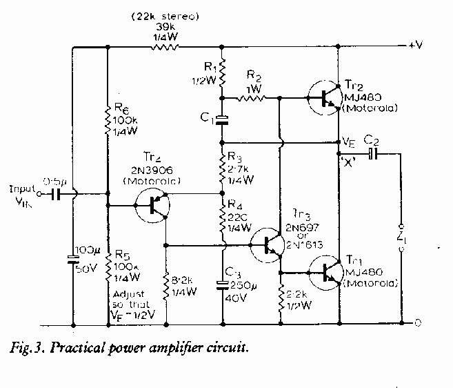
In the context of amplifier design, particularly Class B amplifiers, the operational characteristics and design considerations are crucial for achieving optimal performance. Class B amplifiers utilize a push-pull configuration, where two complementary transistors (NPN and PNP) amplify the positive and negative halves of the input signal, respectively. This configuration is advantageous due to its high efficiency, as each transistor conducts for only half of the input waveform, minimizing power dissipation during idle conditions.
However, the design must carefully consider the matching of the transistors in the push-pull pair. Dissimilarities in the characteristics of the transistors can lead to crossover distortion, which occurs during the transition between the two conduction states. This distortion is particularly noticeable at low output levels when one transistor turns off and the other turns on. To mitigate this issue, biasing techniques such as class AB operation can be employed, where a small bias current keeps both transistors slightly on, reducing the crossover region and improving linearity.
Another critical aspect of Class B amplifiers is the power supply design. The output current demand from the transistors increases with the output signal, which can lead to voltage drops across the power supply rails if not adequately designed. This situation can worsen the smoothing of the power supply, resulting in ripple and potential degradation of audio performance. To address this, adequate power supply decoupling and regulation must be implemented to ensure stable voltage levels during operation.
In summary, while Class B amplifiers offer significant advantages in terms of efficiency and low static power dissipation, careful attention must be paid to the matching of the output transistors and the design of the power supply to minimize distortion and ensure consistent performance. Proper biasing and power supply design are essential for optimizing the operation of these amplifiers in various applications, including audio amplification and signal processing.The major advantage of amplifiers of this type is that the normal static power dissipation is very low, and the overall power-conversion efficiency is high. Unfortunately there are also some inherent disadvantages due to the intrinsic dissimilarity in the response of the two halves of the push pull pair (if complementary transistors are used in asymmetrical circuit arrangement) together with some cross-over distortion due to the I c /V b characteristics.
An additional characteristic of the class B output stage is that the current demand of the output transistors increases with the output signal, and this may reduce the output voltage and worsen the smoothing of the power supply, unless this is well design 🔗 External reference
Related Circuits
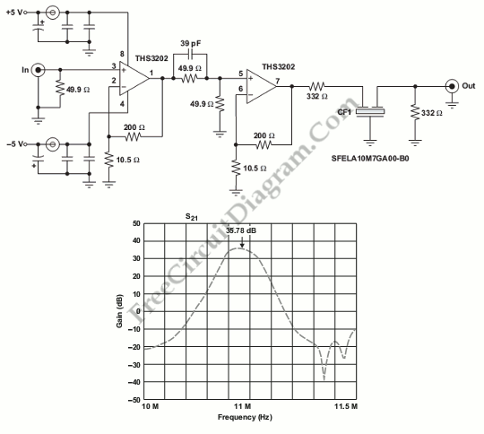
This is a 10.7-MHz intermediate frequency (IF) amplifier circuit. This circuit is utilized in various applications such as cell phone base station receivers (final IF) and FM broadcast receivers. The 10.7-MHz IF amplifier circuit is a crucial component in radio...
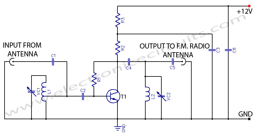
This FM booster allows for clear reception of programs from distant FM stations. The circuit features a common-emitter tuned RF preamplifier utilizing the VHF/UHF transistor 2SC2570 (only labeled as C2570 on the transistor body). The input coil L1 is...
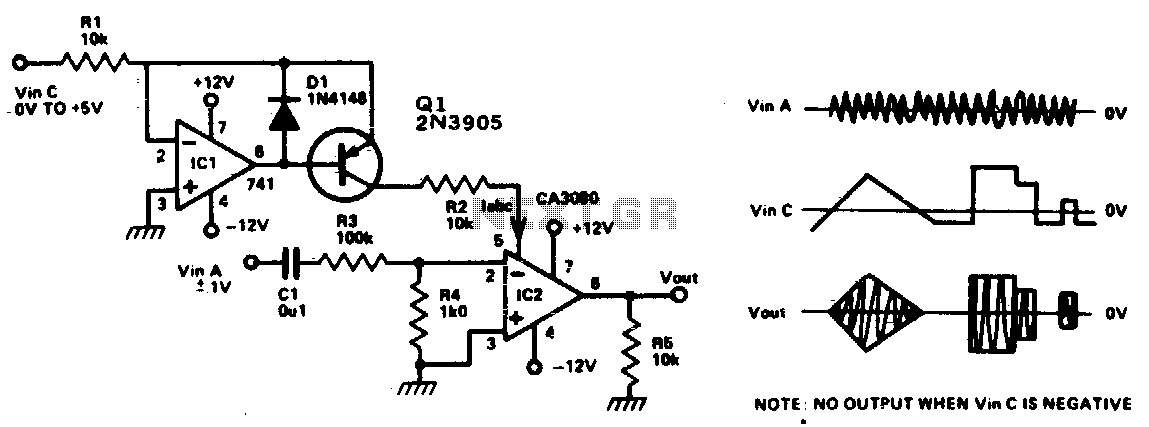
This circuit is essentially an operational amplifier (op-amp) with a differential input voltage of ±10 mV between pins 2 and 3, along with an additional input at pin 5. A current (Iabc) is injected to control the current at...
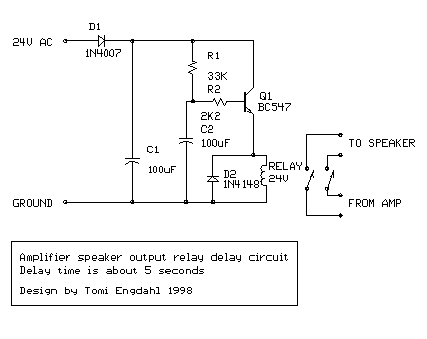
This is a simple circuit designed for an audio amplifier project to control the speaker output relay. The purpose of this circuit is to manage the relay that activates the speaker output in the audio amplifier. The circuit is...
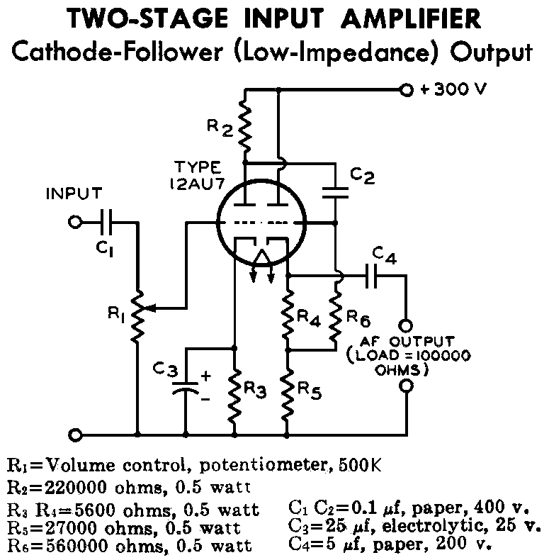
12AU7 (ECC82) Cathode Follower Tube Preamplifier Schematic. This is a two-stage 12AU7 preamplifier featuring a low impedance output stage. The overall gain is approximately 8 times. The 12AU7 (ECC82) tube is a dual triode commonly used in audio applications due...
The original radio circuitry has been transformed into a block diagram representation. The electrical schematic is illustrated in Figure 1-27, which depicts a typical single-tube amplifier of Group A. One figure represents the audio amplifier circuit for the original...