
100kHz-30MHz active antenna circuit diagram

The design of this active antenna circuit is particularly advantageous for applications requiring a balance between sensitivity and selectivity, especially in environments with varying signal strengths. The choice of components, such as the MPF102 and MPS3866 transistors, is critical for achieving the desired frequency response and amplification characteristics. The implementation of a toroidal transformer (T1) not only facilitates impedance matching but also minimizes losses and enhances bandwidth, making the antenna suitable for a wide range of radio frequencies. The careful selection of capacitor values for C1, C3, C4, C5, C6, and C7 ensures effective filtering and stability of the circuit, while the biasing arrangement with resistors R1-R3 maintains the operational integrity of the FET. Overall, this active antenna circuit exemplifies a well-thought-out balance of performance, cost-effectiveness, and compact design, making it an excellent choice for amateur radio enthusiasts and professional applications alike.100kHz-30MHz active antenna with small size, good performance, making simple, low cost and so on, the most suitable for remote medium wave and short-wave radio reception. As sh own in FIG. High-frequency junction FET Q1 (MPF102) connected as a source follower, the whip antenna ANT1 radio frequency signal picked up by the C1 is coupled to its gate. For the purposes of the low-frequency signal, C1 has a high impedance can be suppressed power grid 50Hz and 100Hz hum interference.
neon NE1 electrostatic charge induction antenna vent let go, in order to protect Q1 not because of excessive accumulation of electrostatic charge and gate breakdown. this is because of the antenna packed in PVC pipe, easily generated by friction when dealing with high electrostatic potential, so that the antenna sensitive to electrostatic charge too much, so the breakdown C1 damage Q1.
biasing resistors R1-R3 to the gate of Q1 2.5V.Q1 biased to the source of the RF output signal after Q2 (UHF transistor MPS3866) to enlarge a load with 100mW output power .Q2 quiescent current of approximately 30-40mA, to maintain good linearity when processing large signal. Gain, its wiper connected to the Q2 emitter circuit of potentiometer R5 to mediate this antenna parallel to C3 from the AC bypass effect.
When R5 mediation is not C3 to bypass position, the minimum voltage gain of Q2, its value is about six times, then 2 times the antenna cable to the overall gain. when the impedance is taken into account, the gain of the output of this circuit is about 36dB.R5 should mediate weak signal reception to the best and lowest Useful gain position to maintain optimum dynamic range.
T1 is wound on a toroidal ferrite core broadband transformer, which determines the bandwidth of the antenna amplifier and play the role of impedance matching, the entire winding impedance ratio of one-third of the tap portion is 9: 1 From Q2 look past the collector. 50-70 ohm antenna input impedance is converted Q1, Q2 into 450-680 ohm, T1 this again converted into 50-75 ohm impedance, so that the output jack connected to the receiver input impedance matching to achieve J1 the resistors R6 inhibition Q2 possible parasitic oscillation DC power supply voltage via a T1 cold side AC-grounded capacitors.
The amplifier -3dB bandwidth of about 10MHz, high-frequency low gain, high gain and low-end. This fit the bill because higher frequencies at higher frequency antenna, the required gain is low. In particular, 12MHz and 15Mhz shortwave radio is sometimes very strong signal will cause intermodulation, the antenna gain of the amplifier is not too high. at about 1MHz, the antenna picked up a weak signal, which requires that the amplifier provides high gain.
the low-end amplifier frequency depends on T1, about near 80Hz, it is possible to cover the long-wave AM broadcast band of 140-425. The circuit in Figure dashed box mounted in the shield box, which is a radio frequency antenna signal amplifier circuit .J1 phantom power output by coaxial cable to one end of J2, and then the C4 is coupled to a receiver connected to J3.
Added 13V DC supply voltage of the J2 and J1 by the same length of coaxial cable for the antenna amplifier power, C4 cut off this DC voltage so that it can not enter receiver antenna input circuit. small wall power transformer secondary output of 12-14V AC voltage is applied to socket PL1, half-wave rectified by a diode D1 and R7, R8, C5, C6 after filtered by 13V DC supply voltage .C7 bypassing.
Related Circuits
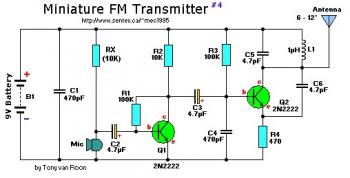
This small FM band transmitter utilizes only two 2N2222 transistors and is capable of transmitting signals up to 1 kilometer away, provided there are no obstacles between the two antennas. The circuit features a microphone preamplifier stage with the...
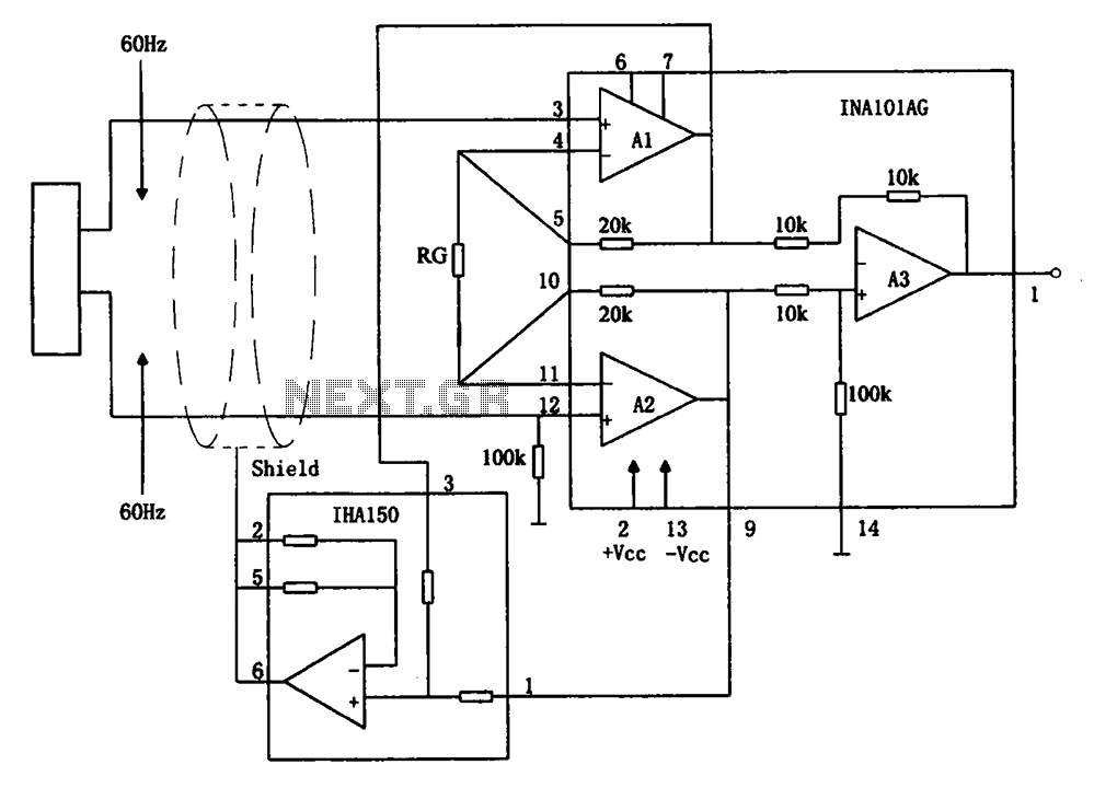
The circuit diagram illustrates a hum elimination instrument amplifier circuit. The amplifier stages A1 and A2 utilize the integrated operational amplifier INA101, followed by stage A3 which employs the INA105. A feedback circuit is incorporated to reduce the power...
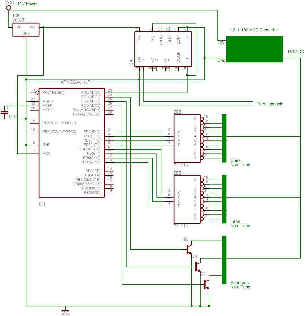
the entire circuit is comprised of integrated circuits. This makes for some easy organization when it goes to the circuit board for soldering. In addition, I used only 3 of the pins on the 3rd nixie tube for the...
A variable gain amplifier is presented. This circuit adjusts the output signal amplitude based on the input signal. The core component is an operational amplifier configured with a negative feedback circuit. By varying the feedback amount, the gain of...
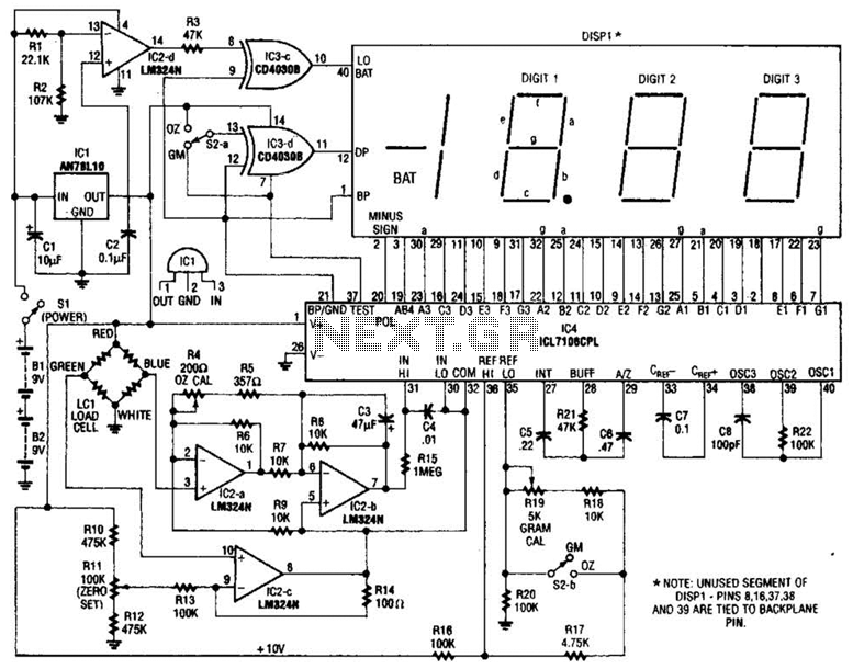
An electronic scale utilizes a pressure transducer (load cell) along with an analog-to-digital (A/D) converter to operate a digital display. The scale's range is determined by the specifications of the load cell, and the display is calibrated in suitable...
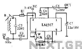
This figure illustrates the schematic of the LM567 SCA broadcast reception information machine. The LM567 serves as a narrow-band phase-locked loop designed primarily for SCA broadcast demodulation. The configuration includes a potentiometer (W) and capacitor (C6) that determine the...