
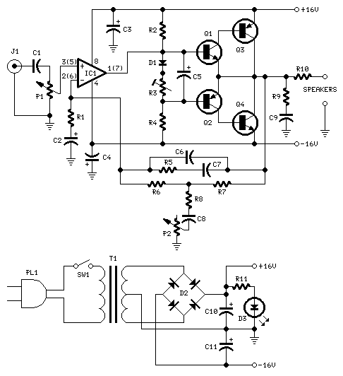
100w audio amplifier
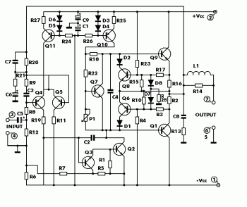
The amplifier circuit described is characterized by its ability to deliver high fidelity audio output, which is critical for audiophiles and sound engineers seeking to reproduce sound as accurately as possible. The high sensitivity of the amplifier ensures that even low-level audio signals can be amplified effectively, making it suitable for a variety of audio applications. The design minimizes power consumption, which is particularly important for battery-operated devices or energy-efficient systems.
The PCB design process begins with the selection of the appropriate software, such as Eagle, which allows for the creation of detailed circuit layouts. The design should include all necessary components, such as resistors, capacitors, transistors, and connectors, arranged in a manner that optimizes space and minimizes signal interference. Once the layout is finalized, printing on high-quality photo or glossy paper is essential to ensure that the traces are accurately transferred during the PCB fabrication process.
After printing, the design is carefully aligned and adhered to the copper-clad board. The application of heat from a hot iron plate activates the toner, causing it to bond with the copper surface. This step is critical as it forms the basis for the etching process, where unwanted copper is removed, leaving behind the desired circuit pattern.
In the absence of a laser printer, utilizing a standard printer and subsequently copying the design onto glossy paper is a viable alternative. This method may require adjustments in the copying process to ensure that the resolution and quality remain suitable for effective etching.
The etching process itself typically involves a chemical solution that removes the exposed copper, resulting in a clean circuit board ready for component soldering. The final PCB can then be populated with electronic components, soldered into place, and tested to ensure functionality and performance in high fidelity audio applications.This amplifier comes with high fidelity (Hi-Fi), high sensitivity, low power consumption and low distortion. It will be nice for your high fidelity sound system. :) Make a PCB in very easy steps. ! Create your PCB design using PCB designer software like Eagle, print out your design on photo paper or glossy paper with laserjet printer.
Stick the pri nted design on the PCB (copper side) and then heat it using hot iron plate. The ink will stick on the PCB and it will be ready for etching process. Note: If you don`t have laserjet printer, then you can print the design on standard paper. Copy the printed design at Copy Service around your location (with glossy paper). 🔗 External reference
Related Circuits
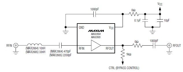
These devices feature a broadband low-noise amplifier (LNA) with an integrated bypass switch. The MAX2664 operates within the UHF frequency range of 470 MHz to 860 MHz, while the MAX2665 functions within the VHF frequency range of 75 MHz...
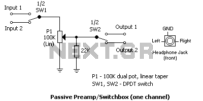
One of the more frequently requested projects on HeadWize has been a switchbox for selecting multiple audio inputs. I built this passive preamp/switchbox several years ago to switch between two stereo sources (a portable FM tuner and portable CD...
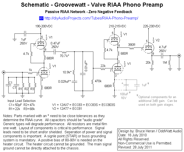
This project has been in development for over a year, initially postponed due to concerns about design complexity and the availability of high-quality phono preamps. The objective was to create a preamp that would deliver performance comparable to commercial...
This design is based on an 18 Watt Audio Amplifier and was developed primarily to address the needs of users who have difficulty locating the TLE2141C chip. It utilizes the commonly available NE5532 Dual IC; however, its power output...
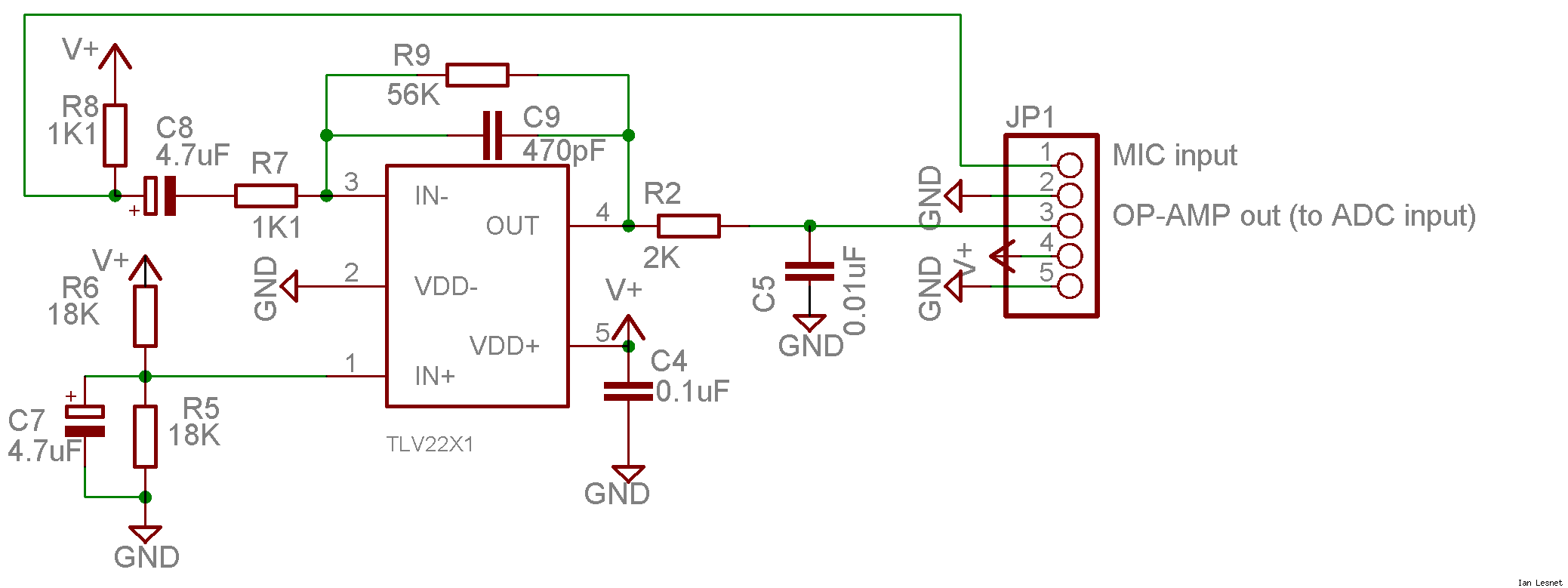
This project utilizes a small, common electret microphone to convert audio into an electrical signal. These inexpensive microphones are typically found in most PC headsets. The output from the microphone must be amplified and zeroed before it can be...
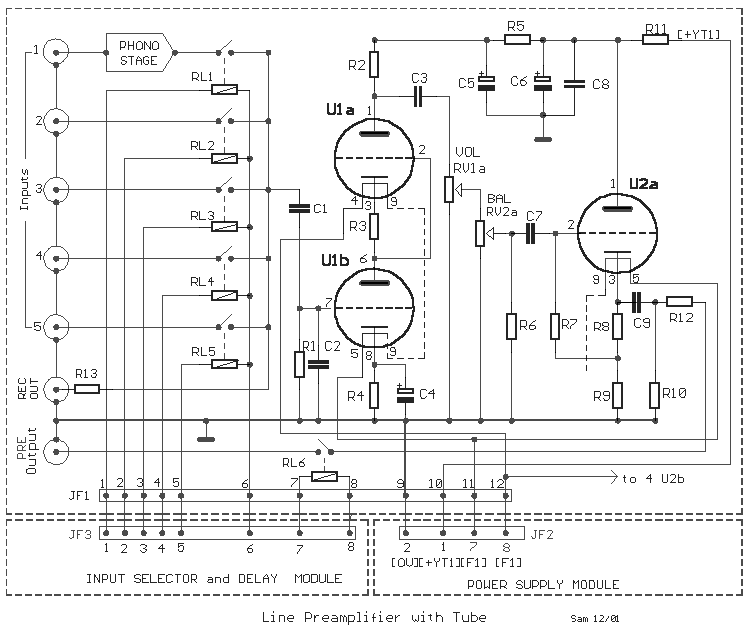
The circuit was designed to create a line preamplifier using double triode tubes. It consists of three parts, including the main preamplifier. The line preamplifier circuit utilizing double triode tubes is structured to enhance audio signals by amplifying low-level signals...