
100W ultra-CPI amplifier circuit
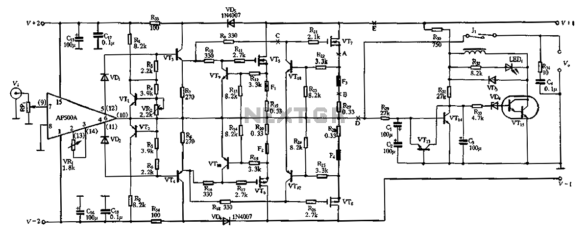
The CPI 100W DC super power amplifier circuit is designed to provide high fidelity audio amplification while maintaining efficiency. The parallel push-pull configuration of the output stage, utilizing transistors VT5, VT6, and VT7, allows for significant power enhancement, effectively doubling the output capability while managing thermal performance. The buffer amplifier stage composed of VT3 and VT4 is critical in driving the output stage, providing the necessary current gain and reducing the potential for distortion.
The circuit's design prioritizes audio integrity by minimizing input signal attenuation through the use of field-effect transistors (FETs). This characteristic ensures that the amplifier reproduces the audio signal with high fidelity, preserving the original sound characteristics. The ultra-CPI bias circuit, comprising components VT1, VT2, RP1, VD1, and VD2, plays a vital role in maintaining consistent performance across varying load conditions. The biasing arrangement allows for precise control over the quiescent current of the output transistors, enhancing linearity and damping performance, which is crucial for high-quality audio reproduction.
The adjustable bias voltage provided by RP2 enables fine-tuning of the output stage's thermal characteristics, allowing the amplifier to adapt to different operating conditions without compromising performance. The inclusion of diode VD1 is a protective measure, ensuring that current flows only in the intended direction, thus preventing any potential damage to the output stage.
Overall, the CPI 100W DC super power amplifier circuit exemplifies advanced engineering in audio amplification, balancing power, efficiency, and sound quality to meet the demands of high-performance audio applications. CPI is 100w DC super power amplifier circuit composed by the AP500. FIG VTs, Vr7 and VT6, VTs parallel push-pull amplifier output stage the composition, to increase the output power. The circuit output power up loow, in order to improve the ability AP500 driven by VT3, VT4 composition of the buffer amplifier stage. In addition to output in parallel to increase the output power, but also reduces the FET input attenuation junction capacitance audio harmonics, the input signal to keep the original sound.
In addition to improving the output of the circuit linearity, improved damping characteristics also have a role in O VTl, VT2, RPi and VDi.VD2 output circuit composed of ultra-CPI bias circuit, the amplifier circuit has a high-quality Class A and Class B high efficiency. fl, VT2 constant voltage bias, the bias voltage can be adjusted to adjust RP2 can change the output transistor quiescent current.
The final output tube circuit quiescent current is adjusted lo ~ 60mAoVDi, f bah to prevent backflow circuit, allowing current to flow only to set direction and allowed to flow in the opposite direction, which ensures super CPI bias circuit in any the case does not appear output MOSFET is off work status o
Related Circuits
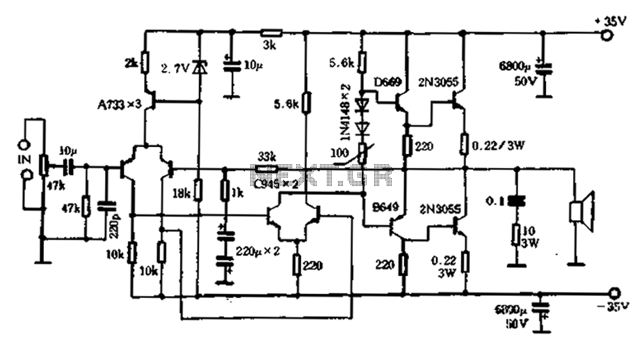
An active high-power tube operates in the MHz range, priced around 3 to 4 yuan, with a transition frequency (fT) exceeding one-fifth of 50 MHz for similar power tubes. This circuit is designed for high reliability in low-frequency high-power...
The LA4440 is a dual-channel audio power amplifier integrated circuit (IC) designed for stereo and bridge amplifier applications. In dual mode, it provides significant audio amplification for various audio systems. The LA4440 audio power amplifier is engineered to deliver high-quality...
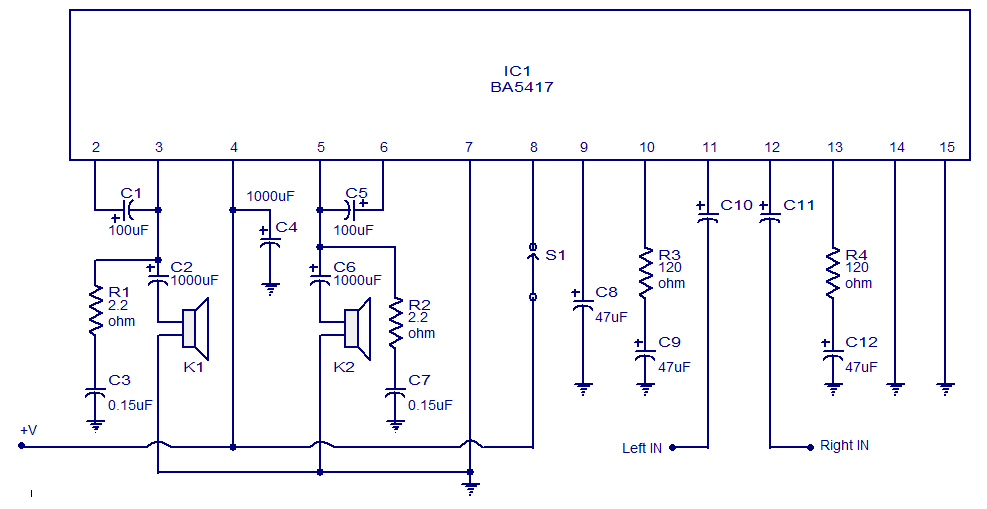
The BA5417 is a stereo amplifier integrated circuit (IC) that features several advantageous characteristics, including thermal shutdown, a standby function, soft clipping, and a wide operating voltage range. It can deliver 5 watts per channel into 4-ohm loudspeakers when...
This circuit consists of a single transistor functioning as an amplifier, providing significant amplification for weak and unipolar signals, which can then be fed into a more powerful amplifier. The described circuit utilizes a single transistor in a common-emitter...
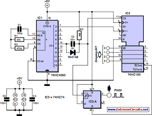
PWM waveforms are frequently employed to regulate the speed of DC motors. The mark/space ratio of the digital waveform can be established either by utilizing an adjustable analog voltage level (as seen in a NE555-based PWM generator) or through...
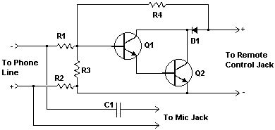
This compact circuit enables automatic recording of phone conversations. It connects to the phone line, the microphone input of a tape recorder, and the remote control jack of the recorder. The circuit detects the voltage level in the phone...