
1024KHz temperature compensation crystal oscillator circuit diagram
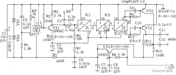
The 1024 kHz temperature-compensated crystal oscillator circuit is designed to provide a stable frequency output that remains consistent despite variations in temperature. Central to this design is a crystal oscillator, which utilizes a quartz crystal to maintain frequency accuracy. The oscillator generates a low-level output signal, which necessitates the inclusion of a transistor buffer stage for signal amplification.
In this configuration, the transistor VT1 acts as a buffer amplifier. The base of VT1 is biased by resistor R2, which sets the operating point and ensures that the transistor remains in the active region for linear amplification. Resistor R3, connected to the collector of VT1, serves as the load resistor, determining the gain of the amplifier and affecting the output signal level. The emitter resistor R4 introduces negative feedback into the circuit, which stabilizes the DC operating point of VT1 and enhances linearity by reducing distortion.
Additionally, the use of a Zener diode in the circuit provides voltage regulation, ensuring that fluctuations in supply voltage do not adversely affect the oscillator's performance. This arrangement allows the circuit to maintain a consistent output frequency of 1024 kHz across a range of temperatures, making it suitable for various applications where precise timing is essential. Overall, this circuit design exemplifies effective use of feedback and amplification techniques to achieve reliable frequency generation.This circuit SJT is 1024kHz temperature compensation crystal oscillator. Circuit theoryis asshown. Because output signal level of the circuit is low, the buffer of follow-up transistor VTl is amplified. VTl base bias resistor R2, the load resistor R3, the emitter resistor R4 are the negative feedback resistors for stablizing VTl DC operating point.
Zener.. 🔗 External reference
Related Circuits
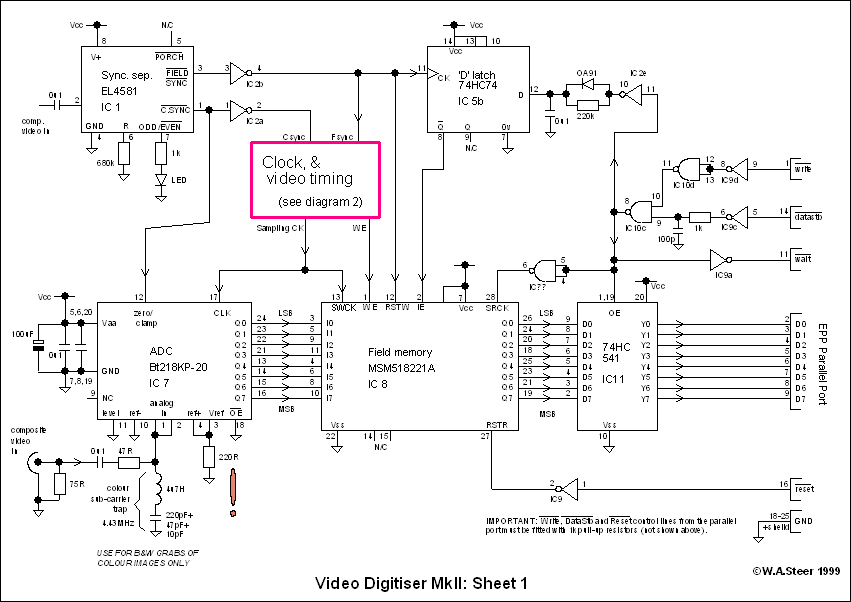
A video digitizer, also known as a frame grabber, captures still picture frames from a television set, video camera, or video recorder, and transmits them to a computer for display, storage, or manipulation. This document outlines the Mark II...

This circuit utilizes one-quarter of an LM3900 to create a simple variable-gain front end for an oscilloscope. R7 serves as the gain control. Additionally, a basic preamplifier is included for applications requiring more than 10X gain. The circuit employs the...
This HD TV UHF wideband amplifier (Ultra High Frequency amplifier) provides a total gain of 10 to 15 dB within the frequency range of 400 to 850 MHz, making it suitable for areas with weak television signals. To ensure...
This circuit will drive a small DC motor over a wide range of speeds without stalling by controlling the duty cycle of the motor, rather than the supply voltage. The described circuit utilizes pulse width modulation (PWM) to effectively control...

This is a 35.3 to 10.7 MHz converter circuit. It converts the 35.3 MHz signal coming from a VHF/UHF tuner down to an FM tuner to decode the TV audio in FM. The 35.3 to 10.7 MHz converter circuit is...
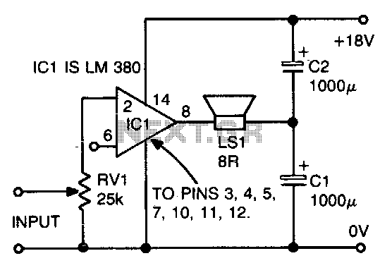
The ground side of the speaker is connected to the junction of two equal high-value capacitors (1000 µF is typical) across the supply. The amplifier output voltage will be Vs/2, and the voltage across CI (if CI and C2...