
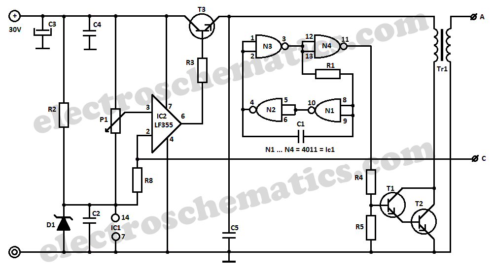
12V 10Amp MJ2955 Switching Power Supply
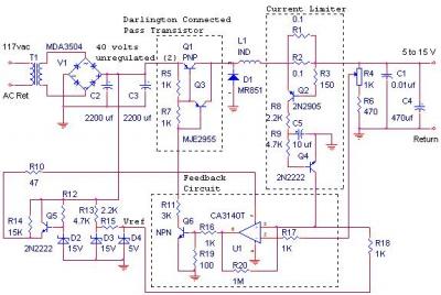
The switching power supply circuit is designed to efficiently convert electrical energy while maintaining a stable output voltage of 12 volts. The core of the design revolves around a discrete transistor regulator, which is complemented by an operational amplifier that serves as a comparator. This configuration ensures that the output voltage is regulated effectively, responding to variations in load conditions.
The absence of an adjustable current limiter is noteworthy; however, the components R1, R2, R3, Q2, R4, R8, R9, C5, and Q4 collectively establish a current limiting mechanism that caps the output at approximately 10 amps. This feature is critical for protecting both the power supply and connected loads from overcurrent conditions.
The inclusion of inductor L1 and diode D1 differentiates this switching power supply from traditional linear designs. L1 serves to smooth out the output current, while D1 provides a path for the inductor current when the switch is turned off, contributing to the overall efficiency of the circuit. The operational amplifier (U1) operates as a comparator, utilizing a small amount of hysteresis to stabilize the feedback loop, thereby enhancing the transient response of the power supply.
A significant aspect of this design is the variable switching frequency that correlates with the output load current. While this feature may introduce unwanted noise and spurious signals, it is a common characteristic in simpler switching power supplies. In contrast, modern designs often employ PWM (Pulse Width Modulation) techniques to maintain a constant switching frequency, which minimizes electromagnetic interference and enhances performance.
The use of a Darlington pair configuration for the pass transistors increases the current handling capability and ensures robustness in the design. This configuration allows for higher gain, which is beneficial in maintaining stable operation under varying load conditions. The internal trim-pot (R4) provides versatility, enabling the adjustment of the output voltage within a range of 5 to 15 volts, accommodating various application requirements.
In summary, this switching power supply design effectively combines traditional linear power supply principles with modern switching techniques, providing a reliable and adjustable voltage source suitable for a variety of electronic applications.The switching power supply provides 12 volts, at 10 amps, maximum, using a discrete transistor regulator with an op-amp functioning as a comparator in the feedback circuit. With reference to the schematic, the front panel power-on light is not shown. There is no adjustable current limiter in this unit, although R1, R2, R3, Q2, R8, R9, C5 and Q4 se t the current limit to approximately 10 amps. As you can see, the design is very similar to that of a linear power supply, except that L1, and D1 have been added, and U1 operates in a switching mode as a comparator with a small amount of hystersis. The switching frequency of this unit varies with the output current drawn by the load. This is an undesireable feature, which is why PWM regulators are used today. With a PWM regulator, the switching frequency is constant and will produce spurs only at known discrete frequencies rather than spurs at all frequencies.
The Darlington-connected pass transistor block in the schematic is there twice (in parallel) for robustness. R4 in an internal trim-pot that can set the output voltage anywhere between 5 to 15 volts. 🔗 External reference
Related Circuits
The current design of a power inverter offers an efficiency of approximately 85% and a power output exceeding 200 watts. This document provides a complete circuit schematic and detailed building procedure for a home-built power inverter. While numerous articles...
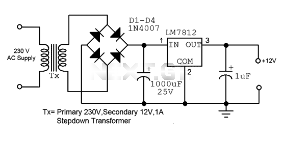
This is a straightforward 12V power supply circuit diagram. It features a fixed voltage output and is based on the LM7812 voltage regulator integrated circuit. The 12V power supply circuit utilizing the LM7812 voltage regulator is designed to provide a...
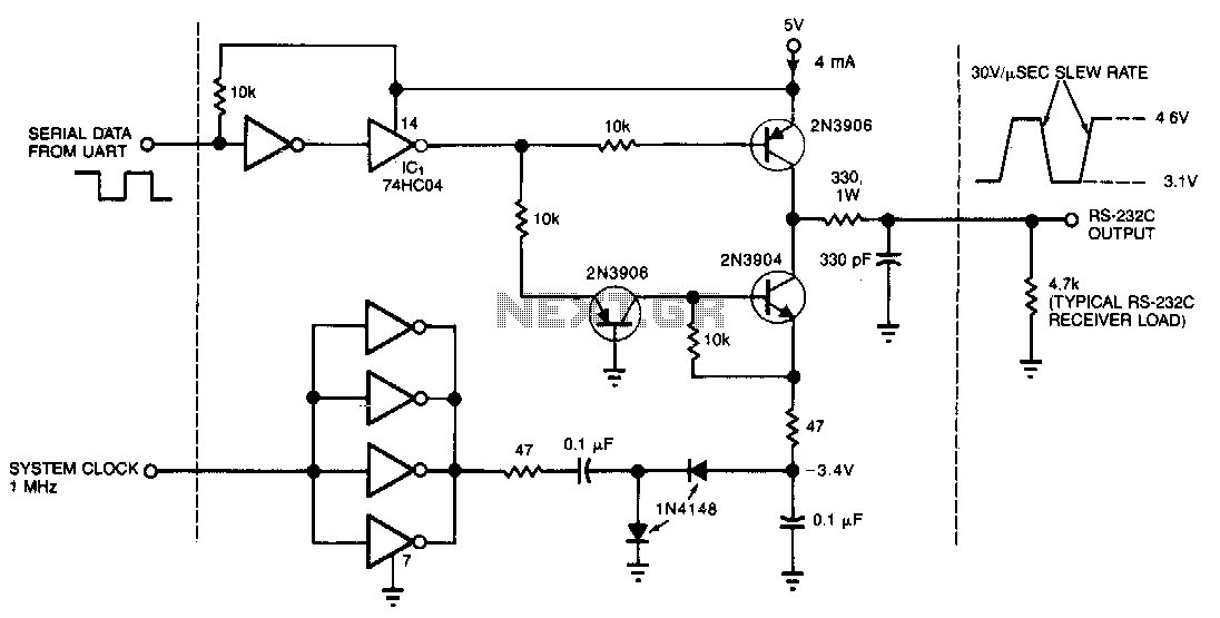
This circuit draws only 4 mA from a 5-V supply while driving a standard RS-232C receiver. The system clock drives a de-de converter that produces -3.4 V. The frequency can range from 0.5 to 8 MHz, but a range...
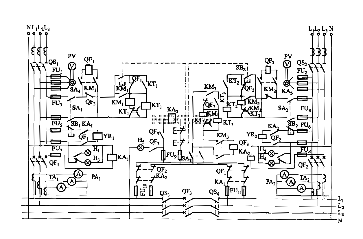
Dual power is provided for each complex, as the load is supplied through a two-way power system. In the event of a power outage, the contact switches transition from a closed position, allowing the power supply circuit to bear...
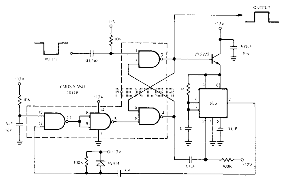
The 555 Timer facilitates a low-loss single-shot circuit and interfaces with the CMOS4011B NAND gate circuit. The standby power consumption is less than 50 µA. When the one-shot circuit is activated, the current consumption is 4.5 mA, and the...
This DIY 12V to 220V DC to AC converter utilizes a CMOS 4047 as its main component, effectively transforming 12V DC into 220V AC. The circuit design of this DC to AC converter primarily revolves around the CMOS 4047 integrated...