
1kHz square wave signal generator

The circuit utilizes the NE555 timer in astable mode, which allows it to generate a continuous square wave output. In this configuration, the frequency of the output signal is determined by the resistor and capacitor values connected to the timer. The formula for calculating the frequency (f) of the output square wave in astable mode is given by:
f = 1.44 / ((R1 + 2R2) * C)
Where:
- R1 is the resistor connected between the discharge pin and the supply voltage,
- R2 is the resistor connected between the discharge pin and the threshold pin,
- C is the capacitor connected between the threshold pin and ground.
In this specific design, the time constant circuit includes a 47 kΩ resistor and a 0.15 µF capacitor. These components establish the timing intervals for the high and low states of the square wave. The values chosen will yield a frequency of approximately 1 kHz.
The NE555 timer operates by charging and discharging the capacitor through the resistors, producing the square wave output at pin 3 of the timer. The duty cycle of the output signal can also be adjusted by varying the resistor values, allowing for flexibility in application depending on the requirements of the circuit being designed.
This type of square wave generator can be utilized in various applications, such as clock pulses for digital circuits, testing equipment, and waveform generation for signal processing tasks. Proper decoupling capacitors should be included in the design to ensure stable operation of the NE555 timer, and a power supply voltage typically in the range of 5V to 15V can be used, depending on the specific requirements of the application.1kHz square wave signal generator As shown by the time base circuit NE555 plus the time constant circuit (47 kfl O.Q15 UF) composed of] hair kHz square wave signal generator.
Related Circuits
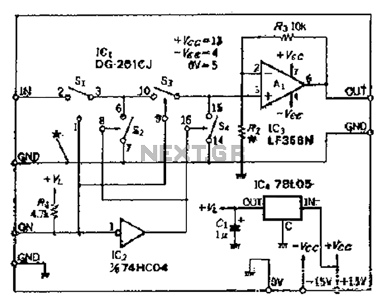
Analog switches SL and SA disconnect the inverted logic signal to terminal 2. S1 and S4 are turned on, allowing capacitance between S1 and S8 to couple. S2 and S4 shunt with an on-state resistance ranging from 50 to...
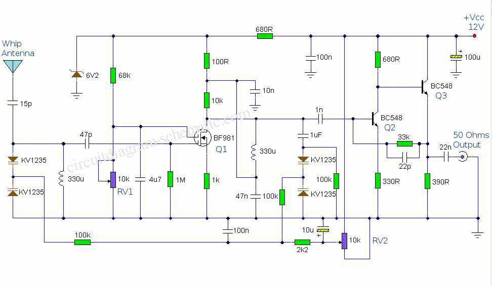
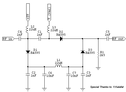
The circuit diagram is designed to enhance the input of a telescopic whip antenna. The preamplifier is intended to operate within the medium waveband, covering frequencies from approximately 550 kHz to 1650 kHz. A tuning voltage is provided through...
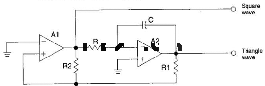
The circuit generates precision triangle and square waves. The output amplitude of the square wave is determined by the output swing of operational amplifier A1, while the ratio of resistors R1 to R2 sets the amplitude of the triangle...
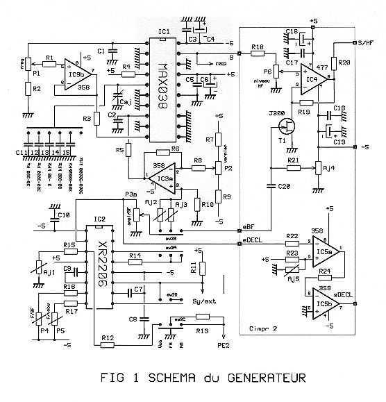
The GHF1 is a small generator covering the HF and LF band from 30 Hz to 30 MHz in 6 ranges. The sinusoidal signal obtained can be amplitude modulated (AM) or frequency (FM). The GHF1 also has a sweep...
This is a PIN diode-based RF signal attenuator circuit that operates with input frequencies ranging from 1 MHz to 500 MHz. PIN diodes are among the most commonly used components in RF applications. The RF signal attenuator circuit utilizing PIN...
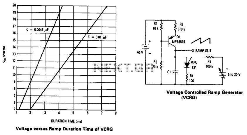
The current source created by Q1 in combination with capacitor C1 determines the duration of the ramp. As the positive DC voltage at the gate varies, the peak point firing voltage of the Programmable Unidirectional Thyristor (PUT) is altered,...