
Cutting good performance signal switching circuit
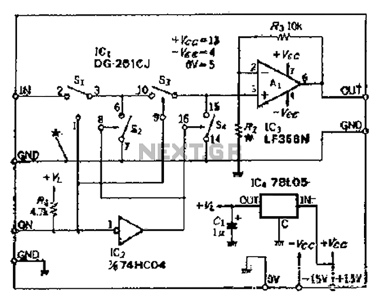
The circuit involves the use of analog switches SL and SA, which are crucial for controlling the flow of signals based on the logic state. When the inverted logic signal is applied to terminal 2, it activates switches S1 and S4, creating a path for capacitance coupling between S1 and S8. This configuration is essential for ensuring that the signals can interact without direct electrical connection, thereby maintaining isolation while allowing for signal transmission.
The on-state resistance of the switches, which is specified to be between 50 and 100 ohms, plays a significant role in determining the overall signal integrity and performance of the circuit. Lower on-state resistance typically results in reduced power loss and improved signal fidelity.
Additionally, the operational buffer amplifier serves to isolate the input from the output, providing a high input impedance and low output impedance. This characteristic is vital for preventing loading effects on the previous stage of the circuit. The choice of resistor R2 should be made considering the availability of components and the desired voltage gain, which is specified as 4.1 +/- 1. This gain setting can be critical for applications requiring specific signal levels, ensuring that the output remains within acceptable limits for further processing or interfacing with other circuit stages.
Overall, the described circuit configuration is designed to facilitate efficient signal management while maintaining the necessary performance characteristics through careful selection of components and design parameters.Analog switches sl and sa disconnect, Ctz the inverted logic signal to terminal 2 s! And 84 is turned on, so that prisoners capacitance between S1 and S 8 and coupling will be generated and S 2 and 8 4 shunt (on-state resistance 50 ~ lOOQ). OP buffer amplifier is a buffer amplifier. Rz need to choose according to the availability of several scrimp 4 1 +/l where the voltage gain.
Related Circuits
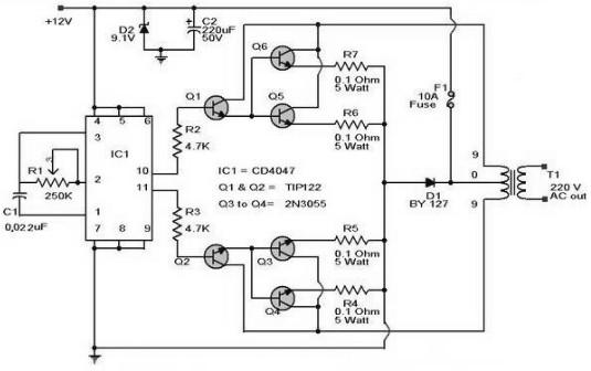
The schematic diagram of a 100W inverter circuit converts a 12V DC input into a 220V AC output. The circuit is built using the IC CD4047 to generate a 50Hz sine wave signal. The power transistor 2N3055 amplifies the...
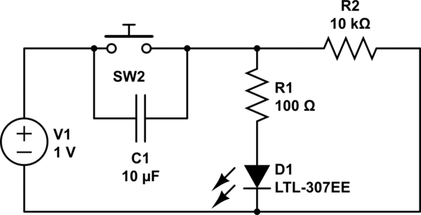
Understand why the LED does not light up, as the capacitor appears to be bypassing the switch. When the capacitor is fully charged, it does not conduct electricity. Although the individual is a beginner, after 20 hours of studying...
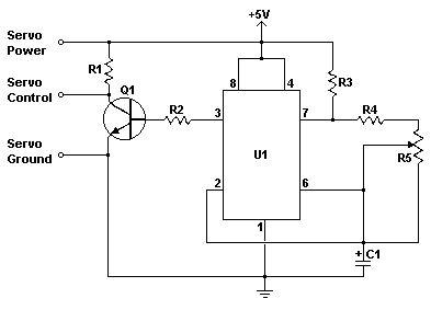
Servo motors are utilized in various applications, including robotics, puppetry, photography, and more. These compact motors can adjust their output shaft to a specified position on command and maintain that position. Most servos offer a range of motion of...
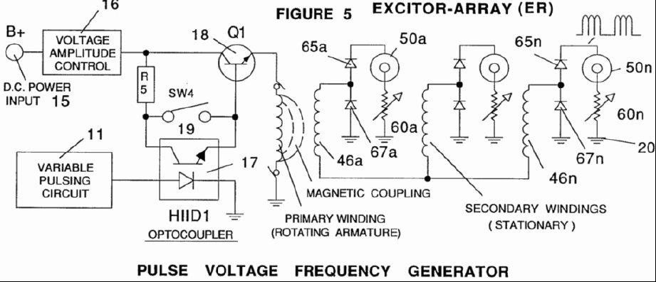
A power supply system utilizes a generator as a source of fuel to separate hydrogen and oxygen gases from natural water. It has the capability to control gas production by varying the amplitude of the voltage and/or the pulse...
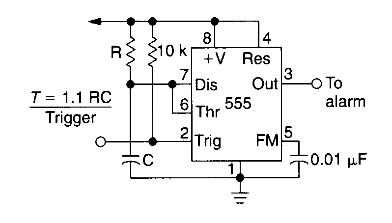
A very regular configuration of the 555 astable timer to work as a timer to trigger an alarm or any other equipment connected to pin 3. R resistor should be replaced with a potentiometer that will change the time...

A series of LEDs that turn on and off in a precise sequence, creating a calming and hypnotic effect. Various LED chaser, scanner, and sequencer circuits exist, utilizing discrete transistors, logic integrated circuits (ICs), or microcontrollers. However, a common...