
2.5A/1.25 To 25V Regulated Power Supply
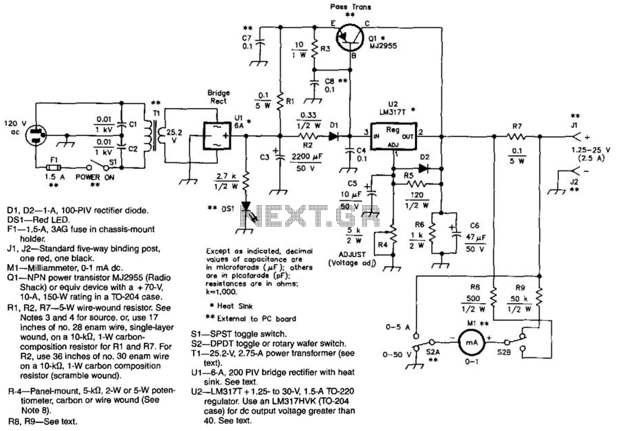
The power supply circuit described integrates an adjustable voltage regulator and a pass transistor to provide a stable output voltage across a variable load. The LM317J regulator is a well-known component in power supply design, offering adjustable voltage capabilities. The MJ2955 serves as a high-power pass transistor, enhancing the current handling capacity of the circuit.
The heatsinking requirements are critical for both the LM317J and MJ2955 due to the significant thermal dissipation that can occur under load. The specified heatsink dimensions ensure that the components operate within safe temperature limits, thereby enhancing reliability and performance.
Resistor selection is also paramount, with R8 and R9 being precision resistors to maintain voltage regulation accuracy. The use of high-quality capacitors, particularly in power supply applications, helps in smoothing the output and reducing ripple voltage, which is essential for sensitive electronic applications.
The inclusion of a milliammeter allows for real-time monitoring of the output current, facilitating adjustments and ensuring that the load does not exceed the rated capacity of the power supply. The toggle switches (S1 and S2) allow for easy operation and configuration of the circuit, while the binding posts (J1 and J2) provide a robust connection for output terminals.
Overall, the circuit design emphasizes reliability, precision, and ease of use, making it suitable for a wide range of applications in electronics. The specified components and layout provide a clear roadmap for constructing a high-performance adjustable power supply. This power supply uses an LM317J adjustable regulator and an MJ2955 pass transistor. Ql and U2 as well as Ul should be heatsinked. A suitable heatsink would typically be 4" 4" 1" fins, extruded type, because up to 65 W dissipation can occur. R8 and R9 should be 1% types or selected from 5% film types with an accurate ohmmeter. Capacitors are disc ceramic except for those with polarity marked, which are electrolytic. D1, D2—1-A, 100-PIV rectifier diode. DS1—Red LED. F1 —1,5-A, 3AG fuse in chassis-mount holder. J1, J2—Standard five-way binding post, one red, one black. M1—Milliammeter, 0-1 mA dc. Q1—NPN power transistor MJ2955 (Radio Shack) or equiv device with a + 70-V, 10-A, 150-W rating in a -204 case.
R1, R2, R7—5-W wire-wound resistor. See Notes 3 and 4 for source, or, use 17 inches of no. 28 enam wire, single-layer wound, on a 10-KOhmhm, 1-W carbon-composition resistor for R1 and R7. For R2, use 36 inches of no. 30 enam wire on a 10-KOhmhm, 1-W carbon composition resistor (scramble wound). R-4—Panel-mount, 5-kfi, 2-W or 5-W potentiometer, carbon or wire wound (See Note 8). R8, R9—See text. 51—SPSTtoggle switch. 52—DPDTtoggle or rotary wafer switch. T1—25.2-V, 2.75-A power transformer (see text). U1—6-A, 200 PIV bridge rectifier with heat sink. See text. U2—LM317T +1.25- to 30-V, 1.5-A 7-220 regulator. Use an LM317HVK (T0-204 case) for dc output voltage greater than 40. See text. 🔗 External reference
Related Circuits
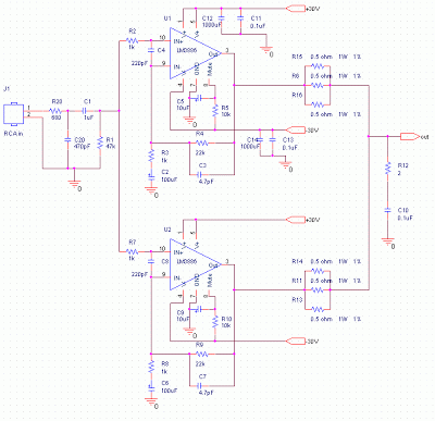
This audio amplifier design employs two LM3886 chips per channel in a parallel configuration, based on the PA100 parallel amplifier detailed in National Semiconductor's application note AN1192. It can deliver approximately 50W into an 8-ohm speaker and 100W into...

National Semiconductor has been designing and manufacturing integrated circuits (ICs) for switch-mode power supplies for many years. The application of these devices is typically straightforward, supported by comprehensive documentation. A common example of a switch-mode power supply is based...
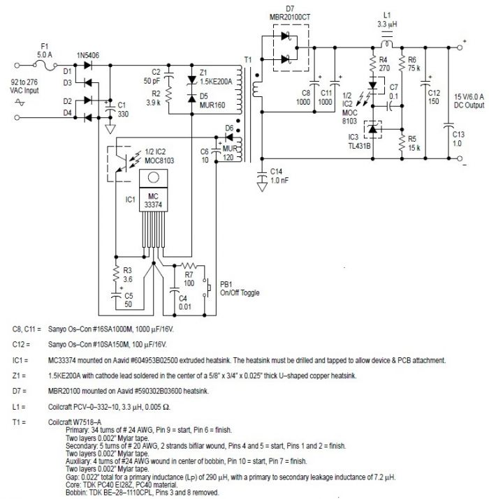
This switching power supply circuit diagram is based on the MC33374 high-power voltage switching regulator IC manufactured by Motorola Semiconductor. The MC33374 switching power supply circuit will provide a maximum output power of around 90 W and requires few...

This current-limiting circuit, illustrated as part of a small bench power supply, can be utilized with any dual-rail current source. The section of the circuit on the left limits the current entering the dual voltage regulator (IC4 to IC7)...
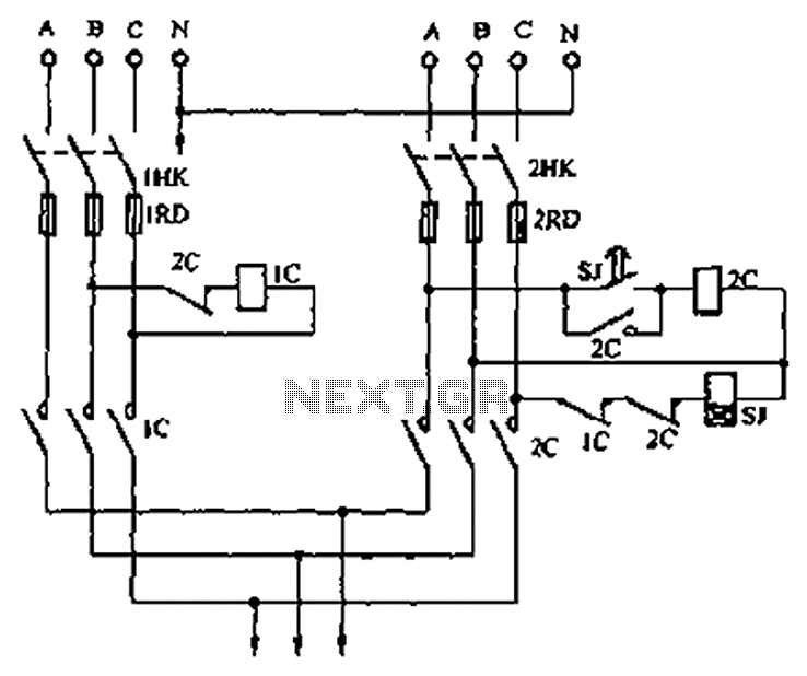
A dual three-phase power line circuit is illustrated in the figure. When the knife switches 1HK and 2HK are closed simultaneously, the normally closed contact 1C disconnects the power supply to the time relay SJ, allowing power to reach...
Circuit diagram of marine TV dish. Circuit diagram of marine TV dish, circuit diagram of marine TV dish, 12V DC to 120V AC inverter circuit diagram PDF, 12V DC to 120V AC inverter circuit diagram PDF. The circuit diagram for...