
250Watt sub-woofer amplifier
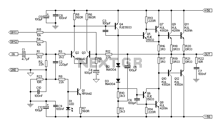
This circuit describes a 300W subwoofer power amplifier designed for high-efficiency audio applications. The amplifier uses a conventional long-tailed pair configuration for its input stage, which is critical for maintaining stability during power transitions. The inclusion of a current sink (Q1) ensures rapid stabilization, mitigating the turn-on thump that can occur in audio amplifiers.
The circuit employs a Class-A driver stage with a Miller stabilization capacitor for enhanced linearity, and the output stage is designed to handle substantial power levels, achieving over 150W into an 8-ohm load. The design can be expanded to support 4-ohm loads by adding four additional output transistors, configured similarly to Q9 through Q12, along with 0.33-ohm emitter resistors.
Thermal management is paramount in this design, with recommendations for extensive heatsinking and fan cooling to prevent thermal runaway, especially in high-power applications. The output stage utilizes a bootstrap method for the collector load, enhancing reliability while simplifying the design.
Resistors in the circuit are specified with particular wattage ratings to ensure they can handle the expected power dissipation, with low-value resistors being wirewound types to manage higher currents. The circuit also includes provisions for a Sound Impairment Monitor (SIM) to provide feedback on clipping, ensuring optimal performance during operation.
Overall, this subwoofer amplifier circuit is a robust design aimed at delivering high performance in demanding audio environments, with careful consideration of thermal management and component selection to ensure reliability and sound quality.You will need to go to extremes with the heatsink (fan cooling is highly recommended). It was originally intended for "light" intermittent duty, suitable for an equalised subwoofer system (for example using the ELF principle - see the Project Page for the info on this circuit). Where continuous high power is required, another 4 output transistors are recommended, wired in the same way as Q9, Q10, Q11 and Q12, and using 0.33 ohm emitter resistors.Continuous power into 8 ohms is typically over 150W (250W for 70V supplies), and it can be used without additional transistors at full power into an 8 ohm load all day, every day.
The additional transistors are only needed if you want to do the same thing into 4 ohms at maximum supply voltage!
300W Subwoofer Power Amplifier. The input stage is a conventional long-tailed pair, and uses a current sink (Q1) in the emitter circuit. I elected to use a current sink here to ensure that the amp would stabilise quickly upon application (and removal) of power, to eliminate the dreaded turn on "thump".
The amp is actually at reasonably stable operating conditions with as little as +/-5 volts! Note also that there are connections for the SIM (Sound Impairment Monitor), which will indicate clipping better than any conventional clipping indicator circuit. See the Project Pages for details on making a SIM circuit. If you feel that you don't need the SIM, omit R4 and R15. The Class-A driver is again conventional, and uses a Miller stabilisation cap. This component should be either a 500V ceramic or a polystyrene device for best linearity. The collector load uses the bootstrap principle rather than an active current sink, as this is cheaper and very reliable.
All three driver transistors (Q4, 5 & 6)must be on a heatsink, and D2 and D3 should be in good thermal contact with the driver heatsink. Neglect to do this and the result will be thermal runaway, and the amp will fail. For some reason, the last statement seems to cause some people confusion - look at the photo below, and you will see the small heatsink, 3 driver transistors, and a white "blob" (just to the left of the electrolytic capacitor), which is the two diodes pressed against the heatsink with thermal grease.
C11 does not exist on this schematic, so don't bother looking for it. It was "mislaid" when the schematic was prepared, and I didn't notice until someone asked me where and what it was supposed to be. Sorry about that. It is in the output stage that the power capability of this amp is revealed. The main output is similar to many of my other designs, but with a higher value than normal for the "emitter" resistors (R16, R17).
The voltage across these resistors is then used to provide base current for the main output devices, which operate in full Class-B. In some respects, this is a "poor-man's" version of the famous Quad current dumping circuit, but without the refinements, and in principle is the same as was used in the equally famous Crown DC300A power amps.
Although I have shown MJL4281A and MJL4302A output transistors, because they are new most constructors will find that these are not as easy to get as they should be. The alternatives are MJL3281/ MJL1302 or MJL21193/ MJL21194. Note: It is no longer possible to recommend any Toshiba transistors, since they are the most commonly counterfeited of all.
The 2SA1302 and 2SC3281 are now obsolete - if you do find them, they are almost certainly fakes, since Toshiba has not made these devices since around 1999~2000. Use a standard green LED. Do not use high brightness or other colours, as they may have a slighty different forward voltage, and this will change the current sink's operation - this may be a miniature type if desired.
The resistors are all 1/4W (preferably metal film), except for R10, R11 and R22, which are 1W carbon film types. All low value resistors (3.3 ohm and 0.33 ohm) are 5W wirewound types. Because this amp operates in "pure" Class-B (something of a contradiction of terms, I think), the high frequency distortion will be relatively high, and is probably unsuited to high power hi-fi.
At the low frequency end of the spectrum, there is lots of negative feedback, and distortion is actually rather good, at about 0.04% up to 1kHz. My initial tests and reports from others indicate that there are no audible artefacts at high frequencies, but the recommendation remains.
Power Dissipation Considerations I have made a lot of noise about not using this amp at 70V into 4 ohms without the extra transistors. A quick calculation reveals that when operated like this, the worst case peak dissipation into a resistive load is 306W (4Ω/70V supplies).
The four final transistors do most of the work, with Q7 and Q8 having a relatively restful time (this was the design goal originally). Peak dissipation in the 8 output devices is around 70W each. Since I like to be conservative, I will assume that Q7 and Q8 in the updated schematic shown contribute a little under 1A peak (which is about right).
This means that their peak dissipation is around 18W, with the main O/P devices dissipating a peak of 70W each. The specified transistors are 230W, and the alternatives are 200W, so why are the extra transistors needed?
The problem is simple - the rated dissipation for a transistor is with a case temperature of C. As the amp is used, each internal transistor die gets hot, as does the transistor case - the standard derating curves must be applied. Add to this the reactive component as the loudspeaker drives current back into the amp (doubling the peak dissipation), and it becomes all too easy to exceed the device limits.
🔗 External reference
Related Circuits
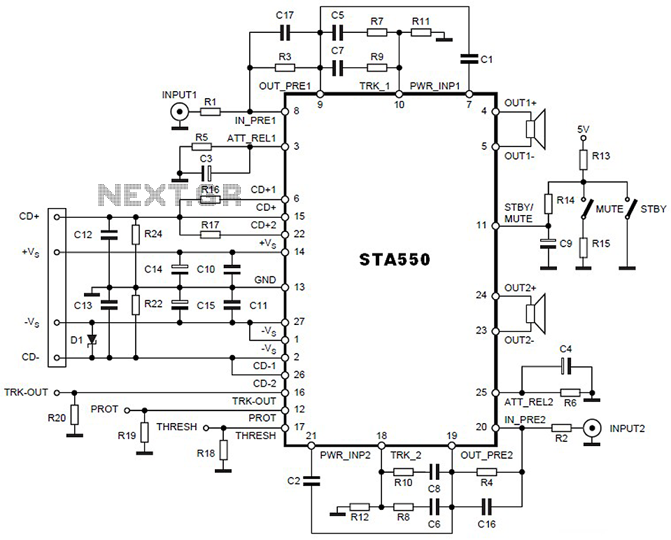
This is a 2 x 70W audio power amplifier circuit built using a single IC STA550. The amplifier circuit requires a few external components, primarily resistors and capacitors, and is straightforward to design. The STA550 audio amplifier can provide...
In a lot of cars, the car radios use amplifiers that their output power does not exceed the 5W with enough distortion in the limits of power. The problem is tied with the utilization of external amplifiers, that will...
This circuit design for an amplifier was created to address the gap in the 3-10 Watts power output range of audio amplifiers available in RED Free Circuit Designs. A straightforward, low-component-count amplifier was developed based on the successful 45...

This notch filter is beneficial for tunable band-reject applications in the audio range. The specified values will provide a tuning range of approximately 300 to 1500 Hz. The notch filter is designed to attenuate a specific frequency while allowing others...
This project is finalized, that means it is no longer experimental. This amplifier, although limited in output power (20W), has been designed to give the best listening pleasure. No compromise has been made during components choice: the 845 output...

A small amplifier with nice characteristics: Tendency of catering: 15V. Force of expense: 4.2Wrms in the 4W. Minimal signal of entry: 94mVp-p with preamplifier, 0.65Vp-p without the preamplifier. More: Materially: R1=2.2kΩ R2=330kΩ R3=4.7kΩ logarithmic potentiometer R4=330Ω R5=1kΩ R6=1.5Ω C1,...
Warning: include(partials/cookie-banner.php): Failed to open stream: Permission denied in /var/www/html/nextgr/view-circuit.php on line 713
Warning: include(): Failed opening 'partials/cookie-banner.php' for inclusion (include_path='.:/usr/share/php') in /var/www/html/nextgr/view-circuit.php on line 713