
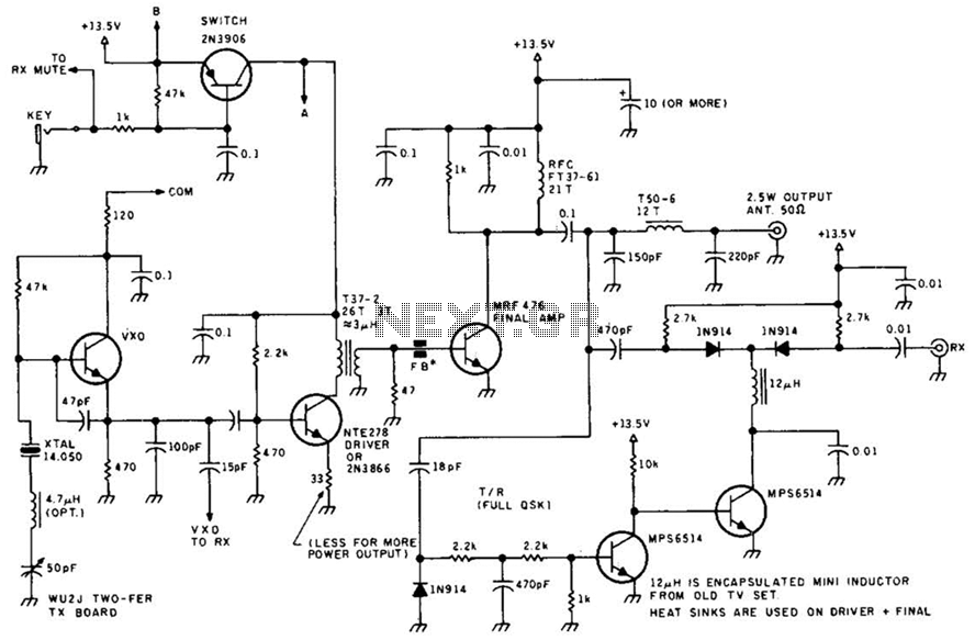
2M Transmitter
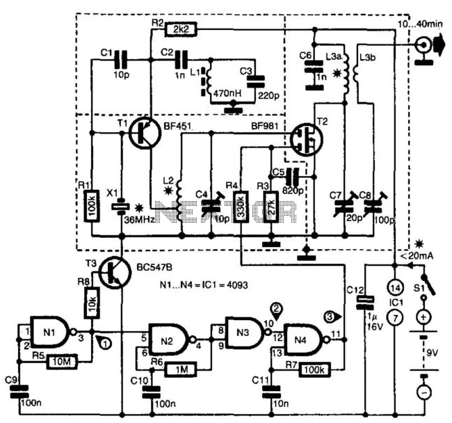
The transmitter circuit is structured to ensure optimal performance for amateur radio applications, with a focus on signal integrity and efficient power consumption. The oscillator stage, utilizing transistor T1 and crystal X1, is critical for generating a stable frequency of 36 MHz. The filtering elements, L1 and C3, are strategically placed to eliminate any potential interference at the fundamental frequency of 12 MHz, ensuring that only the intended harmonics are transmitted.
The tuning circuit L2/C4 is essential for aligning the output to the fourth harmonic frequency of 144 MHz, which is commonly used for radio beacons. The buffer stage, featuring the double-gated FET T2, plays a vital role in isolating the oscillator from the antenna load while allowing for modulation through the second gate. The low output power of 10 to 40 mW is adequate for beacon transmission, providing a balance between performance and battery life.
The modulating signal generated by oscillator N1 is responsible for turning the transmitter on and off, providing a pulsed output that can be easily distinguished by receiving stations. The switching behavior controlled by transistor T3 allows for a flexible modulation scheme, with a frequency range that can be adjusted based on operational needs.
The digital signal shaping at gate N2, combined with the square wave generation, results in a modulated output that can be tailored for various applications. The calibration process involving trimmers C4, C7, and C8 ensures that the transmitter operates at peak efficiency, maximizing output power while maintaining signal quality.
The construction of inductors L2 and L3 from enamelled copper wire is a practical choice, ensuring durability and reliability in the circuit. The specific winding configurations and the emphasis on coupling between L3A and L3B are critical for achieving the desired output characteristics. Overall, the design prioritizes low power consumption, allowing for extended operation from a standard 9-V battery, making it suitable for portable applications in amateur radio. The transmitter was designed specifically for use by radio amateurs as a radio beacon. As such, it provides a good-quality signal that is free of unwanted harmonics. Transistor Tl, in association with crystal XI, operates as a 36-MHz oscillator. Filter L1/C3 obviates any tendency of the circuit to oscillate at 12 MHz (the fundamental frequency of the crystal). Circuit L2/C4 is tuned to the fourth harmonic of the oscillator signal (144 MHz). This signal is fed to the aerial via a buffer stage that consists of T2, a double-gated FET. The (amplitude) modulating signal is applied to the second gate of the buffer. The output power of the transmitter has been kept low, about 10 to 40 mW. The modulating signal is generated by Nl, an oscillator that switches the transmitter on and off via transistor T3.
The switching rate lies between 0.1 and 0.5 Hz. When the output of Nl is low, T3 is switched off, and the transmitter is inoperative because the supply is disabled. When the output of Nl is high, T3 is on and the transmitter operates normally. The digital pattern at the gate of T2 shapes the modulating signal. Gate N2 generates a square wave at a frequency of 0.1 to 1 Hz. As long as the output ofT3 is high, N4 oscillates at a frequency of about 1 kHz. At the relevant gate of N2, there is, therefore, a periodic burst-signal at 1 kHz, and this signal is used to modulate the transmitter.
The digital pattern at the relevant gate of 2 can be varied to individual requirements by altering the values of the feedback resistors in the digital chain. The transmitter is calibrated by setting trimmers C4, C7, and C8 for maximum output power. Inductors L2 and L3 are wound from 0.8-mm diameter enamelled copper wire: L2 = 5 turns with a tap of 1 turn from ground; L3A = 3 turns and L3B = 2 turns.
The coupling between L3A and L3B should be arranged for maximum output power. The circuit draws a current of only 20 mA, which enables the transmitter to be operated from a 9-V battery for several hours. 🔗 External reference
Related Circuits
This circuit enables wireless audio and visual transmission to a television, which serves as a receiver, thus negating the need for a separate monitor. Additionally, it can be connected to a VCR or CCD camera, facilitating the establishment of...
1000 m single-tube FM transmitter circuit diagram of oscillation. The circuit diagram for a 1000 m single-tube FM transmitter is designed to generate frequency modulation signals suitable for transmission over a distance of approximately 1000 meters. This transmitter employs...
This low-power video transmitter is designed for remote control (R/C) applications, surveillance, or amateur radio purposes. It utilizes seven transistors within a crystal oscillator-multiplier RF power amplifier chain, along with a high-level video modulator. A supply voltage of 9...

The circuit diagram of a stereo PLL FM transmitter based on the BH1417 chip is presented. This recent design from RHOM integrates numerous capabilities within a compact package. It features pre-emphasis and a limiter to maintain consistent audio levels...
An FM radio generates an interference signal that can be detected on another FM radio tuned 10.7 MHz higher than the original. A 50 kΩ potentiometer is used to adjust the modulation level to its maximum without introducing distortion....
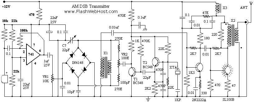
The circuit of AM transmitter is designed to transmit (amplitude modulated) DSB (double side band) signals. A modulated AM signal consists of a carrier and two symmetrically spaced side bands. The two side bands have the same amplitude and...