
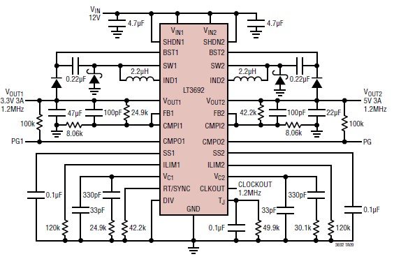
33v and 5v dual tracking regulator using lt3692 dc converter
The LT3692 is designed to facilitate the creation of efficient and compact power supply solutions in various applications. Each channel of the converter operates independently, allowing for flexible voltage outputs tailored to specific needs. The programmable maximum current limit feature is particularly advantageous in preventing overload conditions, ensuring reliability in demanding environments.
The synchronization capabilities of the LT3692 enable multiple converters to operate in unison, which is critical in applications where maintaining a consistent power supply is essential. The internal oscillator's frequency can be adjusted to optimize performance for specific load conditions while minimizing electromagnetic interference (EMI), a common concern in automotive and distributed systems.
The antiphase switching characteristic is a notable design feature, as it effectively cancels out voltage ripple, leading to improved output stability. This is particularly beneficial in sensitive electronic applications where voltage fluctuations can lead to performance degradation or malfunction.
The inclusion of enhanced short-circuit protection ensures that the circuit can withstand fault conditions without sustaining damage, which is crucial for maintaining long-term reliability. The low dropout operation, allowing a maximum duty cycle of 95%, enhances efficiency, particularly in battery-powered applications, where conserving energy is paramount.
In summary, the LT3692 dual current mode PWM step-down DC-DC converter circuit is a versatile and robust solution for generating multiple output voltages with high efficiency and reliability, making it suitable for a wide range of electronic applications.Using the LT3692 dual current mode PWM step-down DC DC converter circuit with two internal 3. 5A switches can be designed a very simple power supply circuit, that can be used for various electronic circuits applications like : distributed supply regulations or automotive circuits. LT3692 provide independent input voltage, shutdown, feedback, soft -start, current limit and comparator pins for each channel. To optimize efficiency and component size, both converters have a programmable maximum current limit and are synchronized to either a common external clock input, or a resistor settable fixed 250kHz to 2. 25MHz internal oscillator. A frequency divider is provided for channel 1 to further optimize component size. At all frequencies, a 180 ° phase relationship between channels is maintained, reducing voltage ripple and component size.
A clock output is available for synchronizing multiple regulators. This DC DC converter circuit presented in this schematic diagram, will provide two independent voltages :3. 3 volts and 5 volt. The maximum output current that can be provided by this DC DC converter electronic project is around 3A for each channel.
As you can see in this schematic circuit, this project require few external electronic parts and needs to be powered from a 12 volt DC power supply. Some features of this DC DC converter electronic project are : independent synchronized switching frequencies, antiphase switching, flexible output voltage tracking, enhanced short-circuit protection, low dropout: 95% maximum duty cycle, low shutdown current: <10 A.
🔗 External reference
Related Circuits
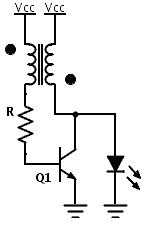
Previously, a boost circuit was tested that enables the powering of a 3 V LED using a discharged battery (approximately 1 V or lower). This circuit consists of a single transistor, one resistor, and a small transformer with a...
Using a switch to power up your microcontroller projects may not be a good idea if you need to "wake" the PIC during some events. For example: A metal detector sends a pulse indicating a car is ready to...
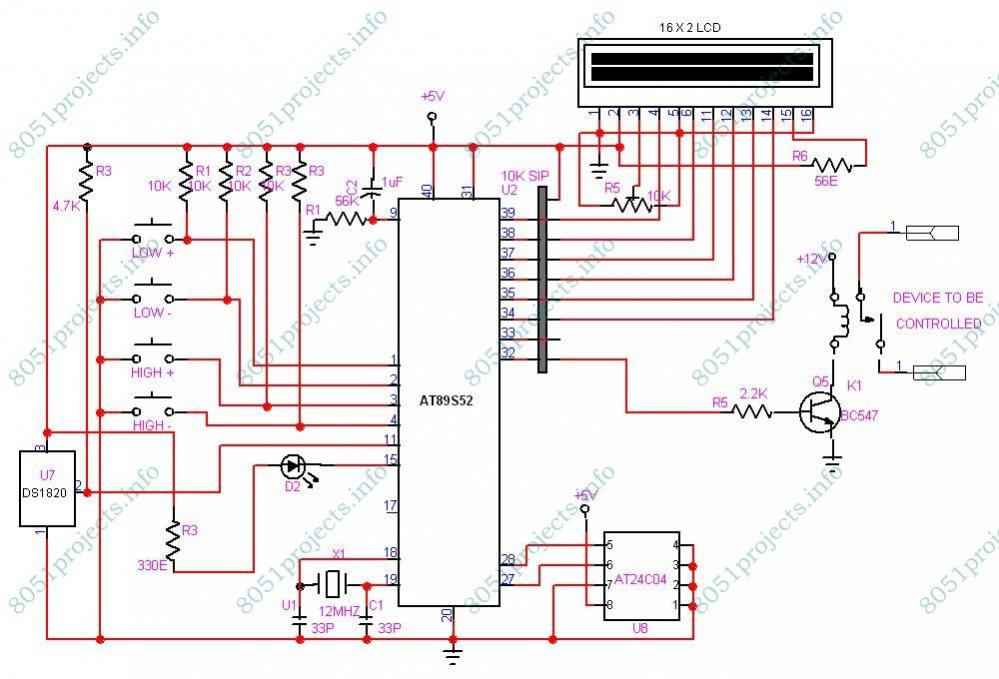
This project is designed to monitor and control temperature. The system utilizes the DS1820 temperature sensor to measure the temperature, which is then displayed on an LCD. It features two preset levels: a low preset and a high preset....
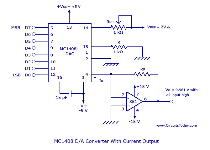
Monolithic/Hybrid Digital to Analog Converters using MC 1408 IC, SE/NE 5018, Specifications and Applications. Monolithic and hybrid digital-to-analog converters (DACs) are integral components in various electronic systems, facilitating the conversion of digital signals into corresponding analog voltages or currents. The...

The term "pentester" refers to a penetration tester, individuals who assess security vulnerabilities. Many high-end hotels globally depend on keycard locks for securing hotel rooms. However, recent incidents of theft have shown that these locks may not be as...
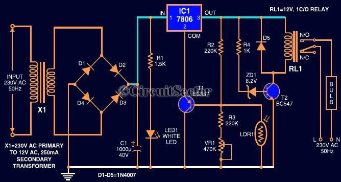
This circuit automates the control of street or porch lights. The automatic lamp controller circuit utilizes a 7806 voltage regulator IC, which can be employed to automate street lights, tube lights, or any other home electrical lighting systems. The...