
380MHz RF2175 linear amplifier circuit diagram

The RF2175 linear amplifier circuit is designed for efficient amplification of radio frequency signals, particularly in applications requiring precise signal integrity and power control. The architecture consists of multiple stages, beginning with a preamplifier that boosts the weak RF signal received at pin 6. This is crucial for ensuring that the subsequent amplification stages can operate effectively without introducing significant noise.
The direct coupling of the internal amplifier to pin 6 enhances signal fidelity, but it also requires careful consideration of the blocking capacitor to prevent any DC bias from affecting the RF signal. The output stage, which is connected to pins 12 and 13, delivers the amplified RF signal, and the interconnection of these pins allows for a combined output that enhances power delivery.
The design incorporates a sophisticated harmonic filtering mechanism at pin 14, which is essential for minimizing unwanted harmonics that could interfere with the desired signal. By employing a resonant filter, the circuit ensures that the second harmonic is effectively shorted, thereby improving the overall spectral purity of the output signal.
Pin 8 serves a dual purpose; it not only enables voltage regulation but also plays a critical role in the operational state of the power amplifier. The ability to control the voltage allows for flexible power management, making the circuit adaptable to varying operational conditions. The inclusion of a high-frequency filter capacitor at this pin further stabilizes the power supply against high-frequency noise, which is vital in RF applications.
Lastly, pin 16's function as VBIAS is integral to the amplifier's efficiency, particularly in low power modes. By ensuring that the proper voltage is applied, the circuit can optimize power consumption while still delivering the necessary performance when full power is required. This versatility makes the RF2175 amplifier suitable for a range of RF applications, including communication systems, signal processing, and other electronic devices that rely on robust RF amplification. As shown in FIG constituted by 380MHz RF2175 linear amplifier application circuit. Radio frequency (RF) signal input from 6 feet, after the preamplifier, after the last stage p ower amplifier output is amplified by 12 and 13 feet. 6 feet and internal amplifier is directly coupled, so plus a blocking coupling capacitor. Output terminals 12, 13 feet and 14 feet are connected inside the chip, usually 12, 13 feet connected together externally as an output signal. 12 and 13 feet as the final stage amplifier power supply terminal, providing a bias current through these pins to the final amplifier.
As the foot 14 of the second harmonic filter circuit using a transmission line or an inductor and capacitor form a resonant filter at 2f0, provide low impedance for the second harmonic, effectively shorting the second harmonic. 8 feet to enable voltage VREG, the pin voltage can be controlled so as to control power supply. When the voltage is low, the power amplifier is turned off; when the voltage is high (2.8V), the power amplifier in the standard working condition.
8-pin external 100pF external high frequency filter capacitor. 16 feet to VBIAS, the foot control efficiency at low power mode circuit, the pin should be set to 2.8V at full power.
Related Circuits
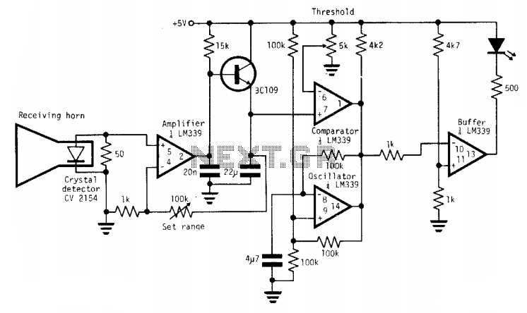
A simple X-band radar detector can indicate changes in RF radiation strength at levels as low as 2 mW/cm². When radiation strikes the detector diode, it generates a voltage at the input of an amplifier. The gain of this...
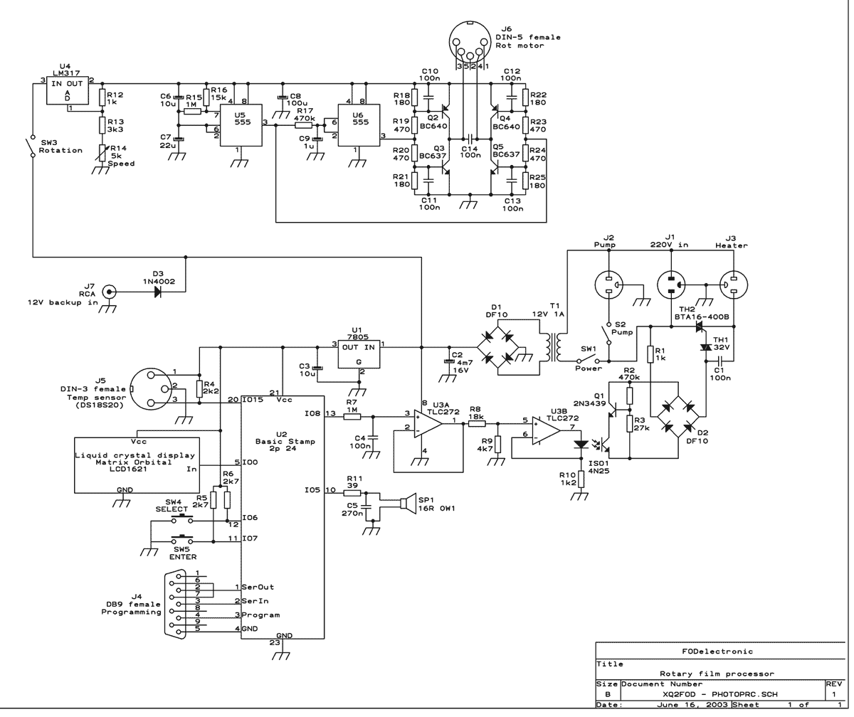
This machine essentially does three things: It controls the process temperature, provides constant agitation of the chemical baths, and performs the timing. The operator must pour in and out the liquids by hand. The heart of the circuit is...
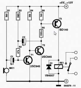
This sound-activated switch allows for control through sound, which can be beneficial not only in robotics but also in home automation applications. The sound-activated switch operates by detecting specific sound frequencies or patterns, typically using a microphone or a sound...
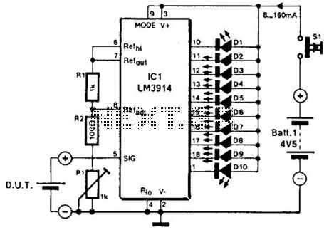
The LM3914A bar graph LED is utilized as a voltmeter for testing batteries. This circuit operates on a 4.5-V battery and compares the battery under test with an internally generated reference, established by resistors R1, R2, and potentiometer P1....
In a lot of cars, the car radios use amplifiers that their output power does not exceed the 5W with enough distortion in the limits of power. The problem is tied with the utilization of external amplifiers, that will...

This is a simple high-frequency signal generator. By changing the inductance of the LC resonant circuit using the band switch S1, the high-frequency oscillation frequency range can be altered. The generator is divided into four frequency stages: the first...