
3W FM Transmitters
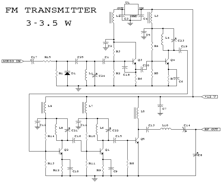
The FM transmitter circuit is designed to operate over a specified frequency range of 90 to 110 MHz, making it suitable for various applications within the FM broadcasting spectrum. The core components of the circuit typically include an oscillator stage, which generates the RF signal, and a modulator stage, where the audio input is combined with the RF signal to create the modulated output.
The output stage of the transmitter is designed to provide the specified power output of 3 to 3.5 watts. This can be achieved through the use of suitable RF transistors or integrated circuits capable of handling the required power levels. The mention of a BLY88 amplifier indicates that this circuit can be further enhanced for higher power applications, as the BLY88 is known for its ability to amplify RF signals effectively.
Incorporating a PLL into the design can significantly improve frequency stability, which is crucial for maintaining clear audio quality and reducing interference with other radio signals. The PLL works by locking onto the frequency of the oscillator and dynamically adjusting it to counteract any drift that may occur due to temperature changes or component tolerances.
The SWR of 1:1.05 indicates a well-matched antenna system, which is essential for efficient power transmission and to minimize signal reflections that could harm the transmitter. An SWR closer to 1:1 is ideal, as it indicates that most of the power is being radiated by the antenna, enhancing the overall performance of the transmitter.
This FM transmitter schematic serves as a foundational design that can be modified and improved according to specific requirements, including power output, frequency stability, and overall performance in a given application.This is the schematic for an FM transmitter with 3 to 3. 5 W output power that can be used between 90 and 110 MHz. Although the stability isn`t so bad, a PLL can be used on this circuit. This is a circuit that I`ve build a few years ago for a friend, who used it in combination with the BLY88 amplifier to obtain 20 W output power. From the notes tha t I made at the original schematic, it worked fine with a SWR of 1 : 1. 05 (quite normal at my place with my antenna). 🔗 External reference
Related Circuits
FM Broadcast Audio Transmitter. The circuit includes a frequency-modulated oscillator, an audio preamplifier with pre-emphasis to provide the frequency-modulating signal, and a buffer amplifier to drive the antenna connector. The FM radio pirate introduction to community radio electronics presents...
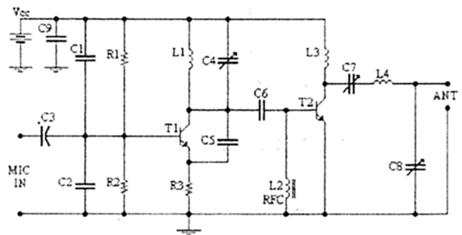
L2 RFC (resistance 1MΩ with an inductor wrapped around it consisting of several coils made from fine insulated wire. The inductor is connected in parallel with the resistance, forming a parallel L-R circuit.) With capacitors C7 and C8, the...

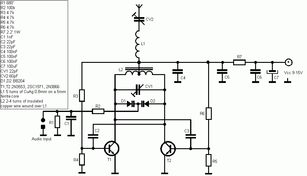
This circuit can be adjusted to operate within the frequency range of 87-108 MHz, achieving a transmission distance of approximately 20 to 30 meters. The design incorporates a pair of BC548 transistors, which, while not specifically designated as RF...
A copy from an old Italian magazine of amateur electronics proposed an add-on for tube receivers. The add-on was a simple one-tube short-wave transmitter leveraging the same power supply already available in the receiver. The project reported in that...
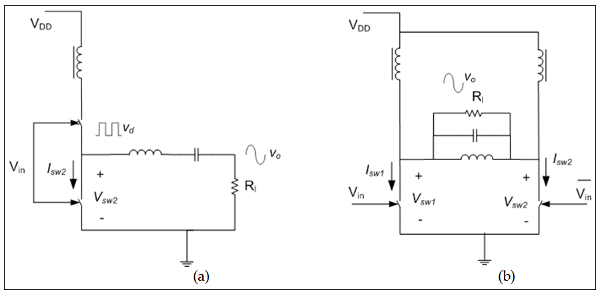
The measured output power and efficiency of a 6 dBm 130nm CMOS class-D inverter chain was analyzed, utilizing gate bias variation to generate a pulse width modulated inverter output voltage (Cijvat et al., 2008). Efficiency versus output power was...
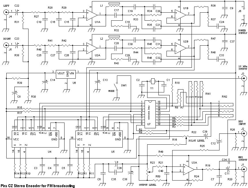
This stereo encoder is a halfway between analogue and digital processing. It combines the best from both domains to provide high-quality and easy to build device. The sampling frequency used in this stereo encoder is 97 times higher than...