
500A power switch control circuit diagram
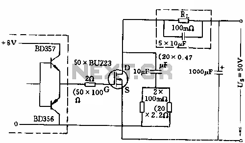
The circuit design utilizes 50 BUZ23 FETs, which are configured in a parallel arrangement to enhance current handling capabilities while maintaining a blocking voltage of 100V. The choice of BUZ23 transistors is significant due to their low on-resistance and high switching speed, which contribute to efficient operation in high-current applications. The minimal control power requirement is a key feature, as it reduces the energy consumption associated with driving the gates of these transistors. This characteristic also mitigates the risk of thermal runaway and second breakdown, which are critical concerns in high-power electronics.
In this configuration, the gate resistance is strategically selected to ensure that the gate drive signals are adequately delivered to all 50 transistors without introducing significant delays or losses. The parallel arrangement allows for the distribution of the gate drive current, thereby minimizing the impact of each individual transistor's gate capacitance on the overall circuit performance.
The inclusion of 20 parallel RC absorption circuits plays a vital role in managing the inductance inherent to the circuit wiring. These RC circuits serve to dampen voltage spikes and transients that can occur during switching events, effectively protecting the FETs from potentially damaging conditions. The RC absorption circuits are designed to absorb excess energy that may be stored in the inductive components of the circuit, ensuring stable operation and prolonging the lifespan of the transistors.
Overall, this circuit design exemplifies a robust approach to managing high currents in a compact form factor while maintaining reliability and efficiency. The careful selection of components and their arrangement is crucial in achieving the desired performance characteristics in high-power applications.The circuit uses 50 BUZ23 field effect transistors connected in parallel, tube blocking voltage of 100V. Required control power is extremely small, and there will be no second breakdown and conduction zone positive temperature coefficient phenomenon.
As the entire circuit current is large, it is where the gate resistance, using the connection element 50 in parallel. In order to load circuit wiring inductance let go of the energy stored in the drain - source access between the 20 parallel RC absorption circuit elements.
Related Circuits
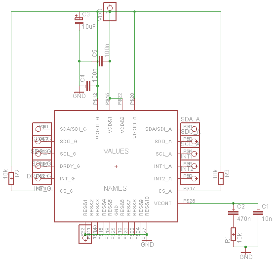
Establish communication between the microcontroller unit (MCU) and the accelerometer using either I2C or SPI protocols. It has been noted that shorting the phase-locked loop (PLL) filter input in the device does not affect the readings from the gyroscope...
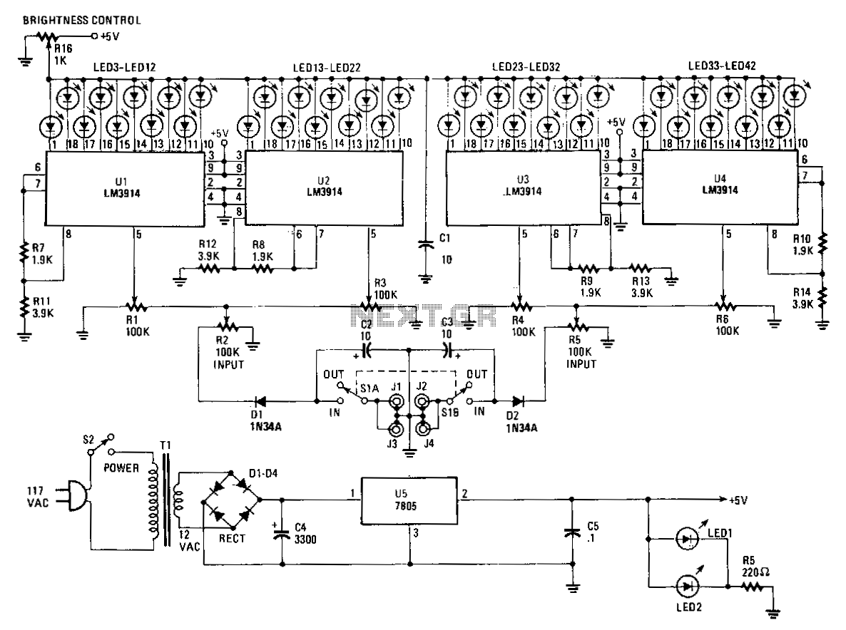
The Stereo Power Meter consists of two identical circuits and a power supply. Each circuit features two LM3914 display chips, which include 10 voltage comparators, a 10-step voltage divider, a reference voltage source, and a mode-select circuit that allows...
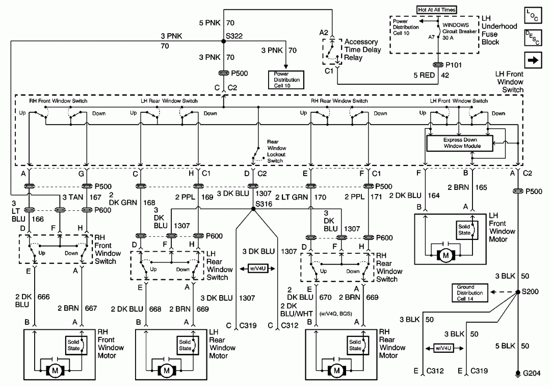
The system utilizes a single circuit breaker instead of fuses. According to the schematic, switches provide 12 volts of power and ground to the window motors in opposite polarities, allowing the windows to move up and down. Troubleshooting should...
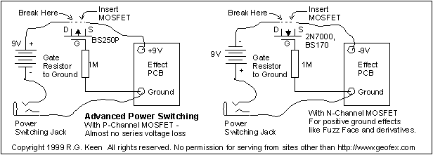
If you are an effects builder or repairer, you know that it is a good idea to protect the circuitry in the effect from the consequences of a reversed battery. While many older effects can withstand a momentary reversal,...
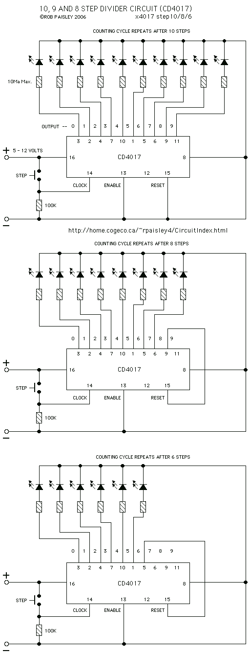
Each time switch S1 is closed the count on the CD4017 advances by 1 step and the corresponding LED turns on. When the maximum count plus 1 is reached for each circuit the cycle is restarted and repeats. The circuit...
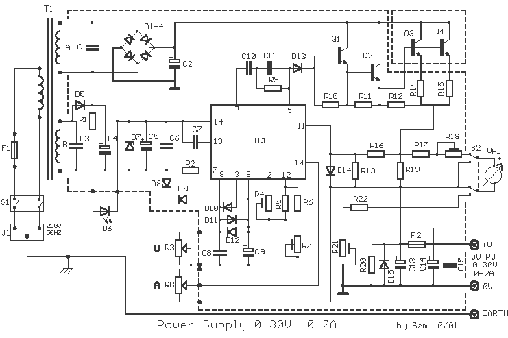
The basic requirements for a laboratory power supply are to provide the necessary voltages and currents with low output resistance, low noise, minimal ripple, and good stabilization. These requirements are addressed within the circuit design. Many power supplies incorporate...
Warning: include(partials/cookie-banner.php): Failed to open stream: Permission denied in /var/www/html/nextgr/view-circuit.php on line 713
Warning: include(): Failed opening 'partials/cookie-banner.php' for inclusion (include_path='.:/usr/share/php') in /var/www/html/nextgr/view-circuit.php on line 713