
50Ohm driver

The described circuit functions as a unity gain buffer amplifier, which is essential for interfacing a test generator with external circuitry. The unity gain configuration allows the circuit to provide a stable output voltage that closely follows the input voltage without amplification, while still ensuring that the signal integrity is maintained.
The high input impedance is critical as it minimizes the loading effect on the preceding stage of the circuit, allowing for accurate signal transmission. This characteristic is particularly beneficial when interfacing with high-impedance sources, such as sensors or other signal generators. The output impedance is set at 50 ohms, making it suitable for matching with standard RF and communication systems, which typically operate within this impedance range.
The circuit employs two pairs of emitter followers (Q1, Q2 and Q3, Q4) arranged to provide buffering. Emitter followers are known for their ability to deliver high current gain while maintaining a low output impedance, which is advantageous for driving subsequent stages or loads without significant voltage drop. The cancellation of base-emitter voltages between the pairs of transistors ensures that any thermal drift or variations in transistor characteristics do not adversely affect the overall performance of the buffer.
Additionally, the inclusion of a preset adjustment allows for fine-tuning of the output to eliminate any DC offset that may arise from mismatched transistor parameters. This adjustment is crucial in applications where precision is required, as even small offsets can lead to significant errors in signal processing or measurement.
Overall, this circuit design exemplifies a straightforward yet effective approach to buffering signals with high fidelity, making it suitable for a variety of electronic applications where signal integrity and accurate representation of the input signal are paramount.To buffer a test generator to the outside world requires an amplifier with sufficient bandwidth and power handling capability. The circuit is a very simple unity gain buffer. It has a fairly high input impedance, a 50 ohm output impedance, a wide bandwidth, and high slew rate.
The circuit is simply two pairs of emitter followers. The base emitter voltages of Q1 and Q2 cancel out, and so do those of Q3 and Q4 The preset is used to zero out any small dc offsets jdue to mismatching in the transistors.
Related Circuits
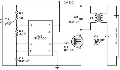
Whenever there is a need for battery-powered lighting, such as for camping, solar-powered cottages, cars, boats, planes, or emergency situations, fluorescent lamps are highly appealing. They are significantly more efficient than incandescent lamps, producing much more light for less...
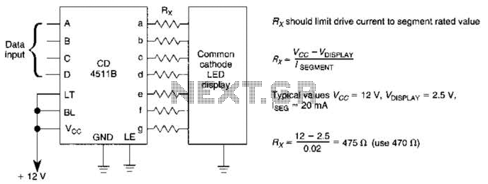
A CD4511B CMOS LED display driver can be utilized to operate a common cathode LED display. Current limiting resistors are employed to restrict the segment current to the specified value at the maximum supply voltage. The CD4511B is a...
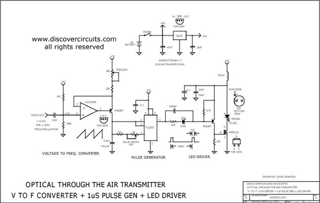
This circuit receives the signal from the amplifier and emits powerful 1μs infrared light pulses from a low-cost LED, which are frequency modulated by the audio information. The 10kHz center frequency of the pulse stream is sufficiently low, allowing...
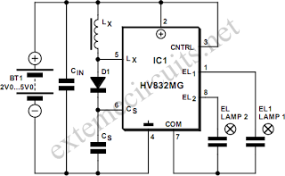
An EL lamp is a solid-state, low-power, uniform area light source. Due to its thin profile (as thin as 0.3 mm) and its capability to be manufactured in various sizes and shapes, EL lamps serve as an ideal solution...
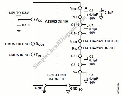
The ADM3251E is a transceiver that features high-speed operation, 2.5 kV full isolation, and a single channel for RS-232/V.28 communication. This device operates from a single 5 V power supply. The ADM3251E transceiver is designed for robust communication in environments...
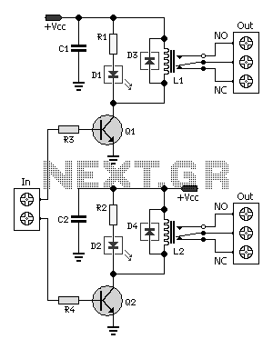
This circuit provides a straightforward and efficient method for interfacing two relays in switching applications. The relay driver utilizes a standard BC547 NPN transistor (or equivalent) to enhance the input impedance. It is a widely used driver capable of...