
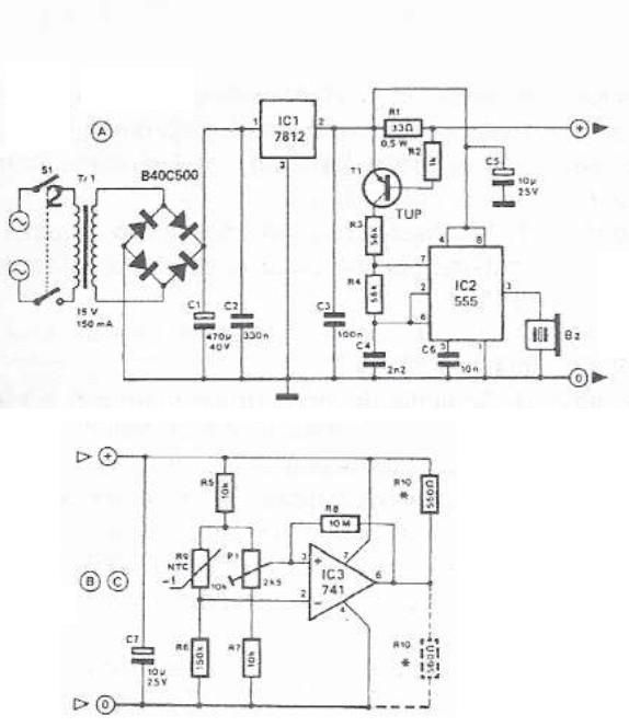
555 Capacitor Tolerance Adjustment circuit
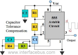
The 555 Timer in astable mode operates as a square wave generator, providing a continuous output signal without the need for external triggering. The frequency of oscillation and duty cycle of the output waveform are determined by the values of R1, R2, and C1, allowing for customization based on application requirements. The timing equation for frequency (f) is given by:
f = 1.44 / ((R1 + 2*R2) * C1)
The duty cycle can be calculated as:
Duty Cycle (%) = (R2 / (R1 + 2*R2)) * 100
This flexibility makes the 555 Timer suitable for various applications, including clock pulses, tone generation, LED flashing, and more. The inclusion of potentiometers R3 and R4 allows for fine-tuning the timing intervals, accommodating variations in component tolerances, and ensuring reliable operation across different conditions. The use of bypass capacitors (C2 and C3) stabilizes the power supply and reduces noise, enhancing the performance of the circuit. It is crucial to select high-quality components to maintain the precision and reliability of the 555 Timer's output, particularly in applications requiring accurate timing.The 555 Timer shown below is configured as an 555 Astable Multivibrator previously discussed. However additional components have been added to enhance the operation of the circuit. As soon as the circuit is powered up the 555 will begin producing a square wave determined by the value of Capacitor C1 and Resistors R1 and R2, as determined by the ti ming equation below. This particular circuit uses a few additional [optional] components to allow for adjustment or compensation for variations in the tolerance of the timing capacitor [C1]. The 555 Integrated Circuit is an extremely accurate device. However it`s output is only as accurate or stable as the external components used. Standard value resistors normally come with a tolerance of either 1% or 5%, of course other resistor tolerances are available.
For more information refer to Resistor Values, Tolerance and Package Sizes. Capacitors on the other hand came in a large variety of tolerances which could change by the quality of the part or by the dielectric used. There are three common capacitor types used with a 555 times, Ceramic, Tantalum, and Electrolytic dielectric.
However regardless of the style used, the best tolerance value will be in the range of 10 to 20%. Also see Capacitor Dielectric Materials and their characteristics. A potentiometer [R3] can be placed on the Threshold pin to adjust the 2/3 Vcc line [recall that the potentiometer will be in parallel with the bottom two 5k resistors]. This effectively changes the trip point of the internal resistor ladder. The additional potentiometer can be used to change the trigger point and be used to compensate for variations in the Trigger Capacitor [C1].
As each new circuit is fabricated and a different capacitor used the potentiometer can be changed to adjust the circuit to compensate for differences in capacitance. The amount of compensation would depend on the values of resistors used in the circuit. Resistor R4 is used to keep the resistance from reaching zero ohms or ground. So the sum of resistors R3 and R4 will be in parallel with the two internal 5k resistors. The capacitor [C3] in parallel with the adjustment resistors is just a by-pass capacitor and is not required.
Capacitor C2 is also a by-pass capacitor. Refer to this page for addition data on Potentiometers. An additional design hint; capacitor values also change with temperature, which this circuit will not compensate for; refer to Film Capacitor Data for additional information. The 555 uses two comparators to control the operation of the timer. The lower comparator is set to trigger at 1/3 Vcc while the upper comparator is set to trigger at 2/3 Vcc.
Three internal 5k resistors placed in series between Vcc and ground are used to provide voltage references. The 1/3 Vcc voltage is generated between the bottom and middle 5k resistors and the 2/3 Vcc voltage is generated between the middle and upper 5k resistors.
The Trigger input [TRIG] is applied to the first comparator which is referenced to the 1/3 Vcc. So as long as the trigger voltage remains above 1/3 Vcc the 555 will not trigger [operate]. The second comparator is referenced to 2/3 Vcc and is used to discharge the timing capacitor C1 once the voltage across the capacitor reaches 2/3 Vcc. In addition to the external capacitor two external resistors are also required to complete the timing circuit.
Resistor [R1 and R2] and the capacitor [C1] form an RC circuit which define the length of time it takes the capacitor to charge [defined by this RC Charging Curve ]. The discharge of the capacitor is completed through resistor R2 [defined by this RC Discharging Curve ].
Before the Trigger pulse occurs [capacitor discharge] the internal transistor is `ON` [conducting] so the capacitor is effectively shorted to ground and is not allowed to charge. Once the trigger is applied and falls below 1/3 Vcc the comparator trips and turns the transistor off.
When 🔗 External reference
Related Circuits
This device can also be referred to as an economical hearing aid, as it can be constructed using low-cost components. Although its performance does not match that of advanced commercially available hearing aids, it can effectively assist individuals with...
The LM339 comparator IC (Integrated Circuit) is utilized to enhance the functionality of electric circuits. A potentiometer (B) is incorporated to adjust the desired setpoint, while a feedback signal is generated by resistor (R). A significant pressure point is...
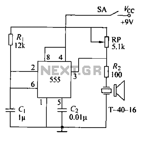
The circuit comprises an ultrasonic transmitter and a T-4 0-16 555 timer circuit. By adjusting the potentiometer RP, the frequency of the oscillation circuit can be modified. The circuit emits ultrasonic signals at a frequency of 40 kHz, with...
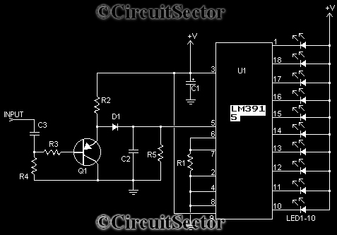
This 555 timer circuit temperature monitoring system project can monitor temperature at up to four points. The system allows for the selection of whether the alarm should be triggered when the temperature increases or decreases, depending on the resistance...

This is a circuit design for a doorbell that produces a bird-like sound. The circuit is controlled by an NPN transistor. The operation of the circuit begins when P1 is set to an experimental value, starting with approximately 220...

The ISO103 ripple reduction circuit features an output circuit combined with an RC high-pass filter designed to filter out output ripple without impacting the direct current (DC) characteristics. Under specific conditions, the circuit is capable of reducing an 800...