
555 car circuit diagram of the device

The circuit utilizes a 555 timer IC in astable mode to generate a continuous square wave signal, which serves as the carrier frequency for the transmission. The selection of components RP1, R1, and C1 is critical as they define the oscillation frequency of the transmitter. Specifically, RP1 and R1 form a voltage divider network that, along with capacitor C1, sets the timing intervals for the oscillation. The output from the 555 timer is coupled to an antenna via capacitor C3, which allows the transmission of the modulated signal.
In the receiver section, the incoming signal is routed through a frequency selective network that filters out unwanted frequencies, allowing only the desired frequency to pass through. The filtered signal is then amplified by the 741 operational amplifier, where the gain is set by the feedback resistor RP2 and the input resistor R2. This gain can be adjusted to optimize the signal for further processing.
The received signal strength is indicated through a series of LEDs (LED1 to LED5). These LEDs light up in sequence as the strength of the received signal increases, providing a visual representation of the signal quality. This feature is particularly useful in applications where monitoring signal strength is crucial for effective communication. The overall design of this circuit is compact and efficient, making it suitable for various applications in wireless communication systems. As shown in the circuit diagram of the device is looking for 555 cars, including a transmitter and a receiver in two parts. The transmitter 555 is a core component of the wave frequency oscillator, the oscillation frequency should be selected than the AM broadcast carrier frequency 535kHz slightly lower frequency value, RP1, C1 is determined by R1, that is, f 1.44/(RP1 + 2R1) C1, L1, C2 form the output resonant circuit, frequency selection, and then by C3 emitted by the antenna. Receiving circuit by the input frequency selective network and 741 op amp, amplifier magnification depends on the ratio RP2/R2s.
LED1 ~ LED5 received signal strength indicator is used, and as the signal strength, the arc tube is lit sequentially.
Related Circuits
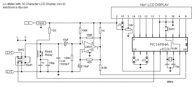
This is one of the most accurate and simplest LC inductance/capacitance meters available, which can be easily constructed by an individual. This LC meter is capable of measuring very small inductances ranging from 10 nH to 1000 nH, 1...
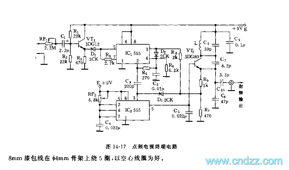
As shown in figure 14-17, this circuit consists of the input circuit, the line frequency synchronization generator, the sample-and-hold circuit, the voltage control delay generator, and the RF modulator. The input circuit includes the input attenuator RP1 and the...
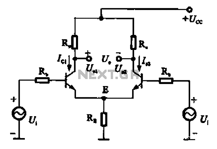
The common mode signal of an emitter-coupled differential amplifier circuit assumes that two equal small increases of the same polarity signal, referred to as the common mode signal, occur simultaneously. This results in an increase in the potential at...

This simple circuit can be used to flash incandescent lamps with a power rating of up to 10W. It is ideal for creating flashing beacons on automobiles and similar applications. The circuit consists of an astable multivibrator utilizing transistors...
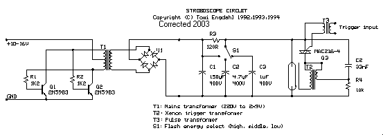
The stroboscope tube requires approximately 250-400V DC for operation. This high voltage is generated by a simple voltage step-up circuit constructed from transistors Q1, Q2, and transformer T1. This circuit outputs about 230V AC, which is then rectified by...
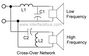
An audio crossover network is utilized within a speaker to separate or filter audio signals of varying frequencies to different speakers inside a speaker cabinet designed for those frequencies. This specific crossover network employs two passive components for each...
Warning: include(partials/cookie-banner.php): Failed to open stream: Permission denied in /var/www/html/nextgr/view-circuit.php on line 713
Warning: include(): Failed opening 'partials/cookie-banner.php' for inclusion (include_path='.:/usr/share/php') in /var/www/html/nextgr/view-circuit.php on line 713