
8-bit bus interface
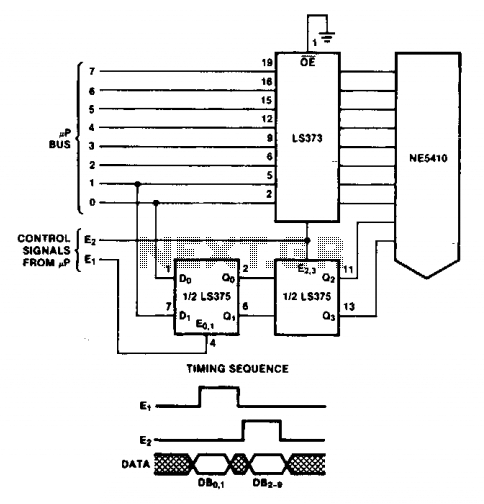
The double latch technique is a critical method in digital signal processing, particularly in applications involving Digital-to-Analog Converters (DACs). This technique allows for stable and reliable data transfer to the DAC, ensuring that the output signal remains consistent until a new data set is provided. The process begins with the valid data being captured by the first latch, which holds the data steady while the second latch is updated with new information.
The timing of the latching process is essential and is influenced by the specifications of the processor being used. Different processors may have varying clock speeds, pulse widths, and timing requirements, which can affect how quickly the DAC can respond to new data inputs. Therefore, it is crucial to synchronize the timing of the E2 pulse with the processor's clock cycle to ensure that the data is latched correctly without introducing errors or glitches in the output signal.
In practical applications, the implementation of the double latch technique requires careful consideration of the circuit design. This includes selecting appropriate components such as flip-flops for the latches, ensuring they can handle the required data rates, and designing the timing circuitry to generate the E2 pulse accurately. Additionally, the layout of the circuit must minimize signal degradation due to noise or interference, which can impact the performance of the DAC.
Overall, the double latch technique serves as an effective means of managing data flow to a DAC, providing a foundation for high-fidelity signal generation in various electronic systems.With this double latch technique, valid data will be latched to the DAC until updated with the E2 pulse. Timing will depend on the processor used. 🔗 External reference
Related Circuits
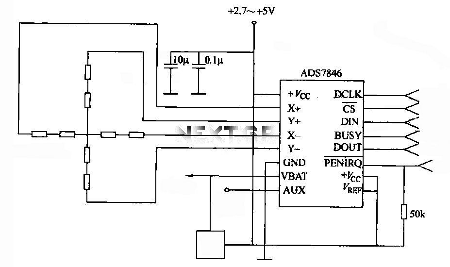
A 4-wire resistive touch screen utilizes an ADS7846 interface circuit. The ADS7846 analog chip incorporates electronic switches and a successive approximation A/D converter. The analog switch chip controls the switching of the X+ (or Y+) positive supply terminal, while...

This design note presents a simple yet feature-rich 16-watt output, universal AC input adapter power supply for modems, hubs, or similar applications. The circuit utilizes a discontinuous mode (DCM) flyback converter topology designed around ON Semiconductor's NCP1027 monolithic current...
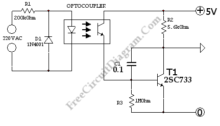
This is a simple 220V power interface circuit. This circuit is used as an interface for monitoring electrical devices and equipment using a computer. The 220V power interface circuit serves as a critical connection point between high-voltage electrical systems and...
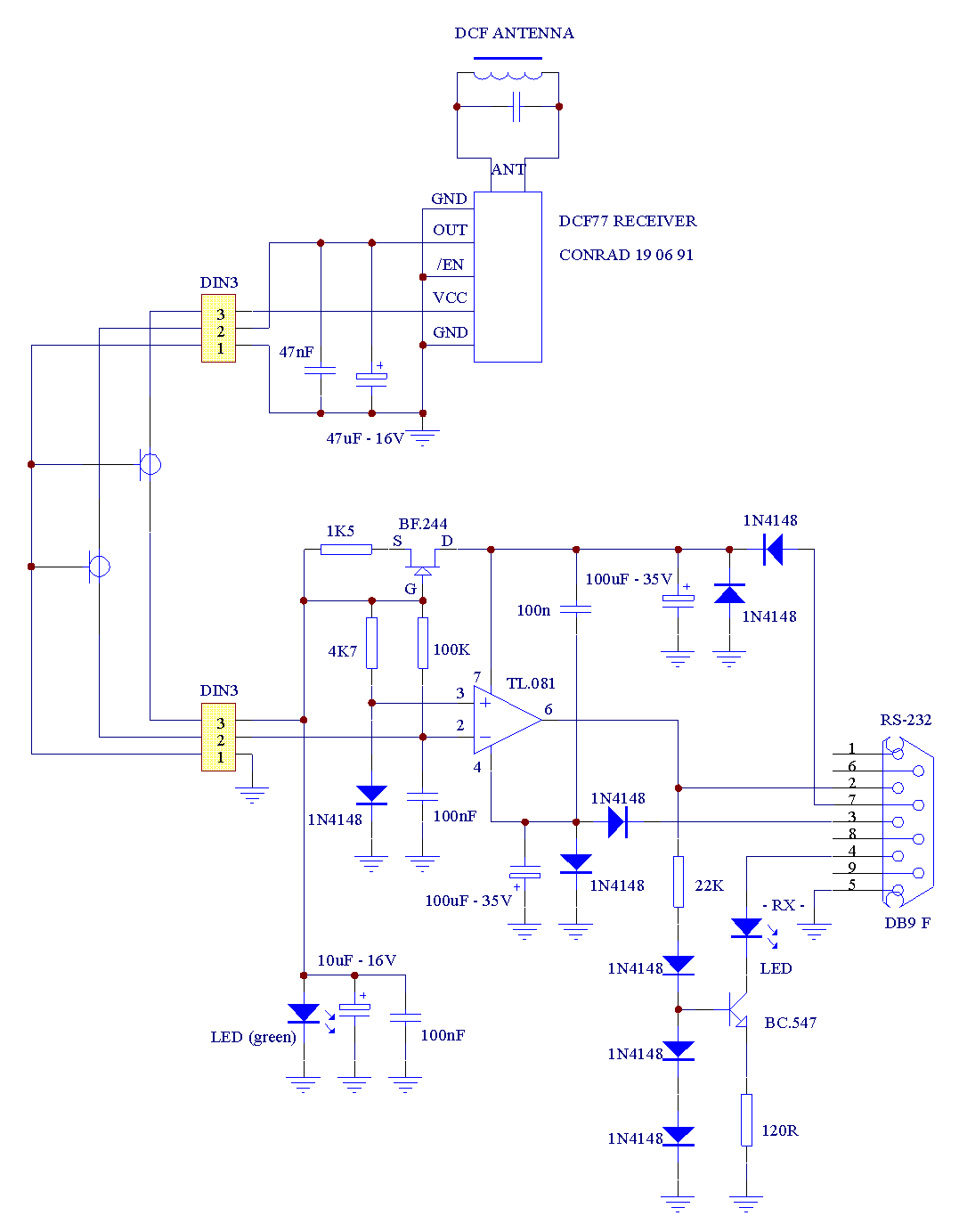
The circuit connects a commercial DCF77 receiver, which is available for approximately $15, to a PC via the RS232 serial port. By modifying the program or the circuit, it is also possible to utilize different systems or I/O ports....
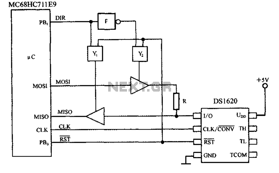
This circuit features a three-wire serial interface for smart temperature sensors, specifically the DS1620, along with an SPI bus interface circuit. The DS1620 is a high-accuracy digital temperature sensor that communicates over a three-wire interface, which consists of a data...

A macro for a register is required for Lab 4, which utilizes a 4-bit bus for data input and a 4-bit bus for data output. This serves as a foundational example for creating similar macros for all components that...