
8 low-pass filter MAX291 TA7504P schematic

The low-pass filter circuit operates by allowing signals below a certain frequency (the cutoff frequency) to pass while attenuating signals above that frequency. The switched-capacitor configuration is particularly advantageous due to its ability to implement precise filtering characteristics without the need for large passive components. The adjustment of the cutoff frequency is accomplished through the modulation of the clock frequency, which directly influences the switching rate of the capacitors, thereby altering the filter's response.
The inclusion of an input attenuator is critical for protecting the circuit from high voltage levels that could potentially cause distortion or damage. Resistors R1 and R2 are carefully selected to provide the necessary attenuation while maintaining signal integrity. The operational amplifier A2 plays a crucial role in maintaining the accuracy of the output by compensating for any drift voltage that may arise due to variations in the input signal or power supply fluctuations. This ensures that the output remains stable and reliable.
Operational amplifier A3 is used not only for smoothing the output waveform but also to enhance the overall performance of the filter by reducing unwanted noise and improving the quality of the output signal. The design of this circuit exemplifies the integration of multiple operational amplifiers to achieve a robust and versatile low-pass filter suitable for various applications in signal processing and communications. Overall, this circuit design demonstrates a sophisticated approach to filtering, enabling precise control over signal characteristics while ensuring high performance and stability. As shown in Figure 8 times the low-pass filter circuit. This circuit uses eight low-pass filter circuit switched-capacitor configuration. Changing the cutoff frequency of the c lock frequency can be changed, and the cutoff frequency of the clock frequency of 1/100. A clock input plus + 5V level square wave signal at A1 input (IN) and output (OUT) terminal properties can be obtained between the low-pass filter. Because the input attenuator and the role of the amplifier output, input and output signal level can reach 10V.
When the supply voltage is + 5V, 9V input voltage peak value or more, for the distortion does not increase sharply in the circuit input signal terminal access R1 and R2 attenuator. Input voltage is 0V, the drift voltage output generated up to 0.4V, for this purpose DC differential between input and output A2 detected and added to A3-inverting input.
Thereby offsetting drift voltage. A3 for smoothing the output of A1 stepped waveform, to enhance its effect. In order to further reduce the output clock pulses may be used in operational amplifier A1 constituting the filter.
Related Circuits
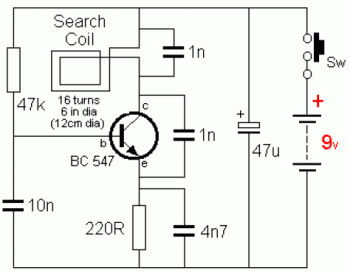
This is a simple and easy-to-build gold detector circuit. The circuit is capable of sensing gold, metal, or coins from a distance of approximately 20 cm, depending on the size of the object being detected. It oscillates at around...
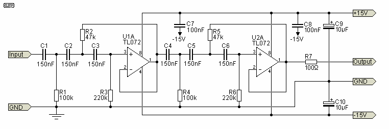
The circuit shown is completely conventional. The Q of the filters has been optimized to allow a higher input impedance than would otherwise be possible, with the final Q of the two filters being almost exactly 0.707 (i.e., a...
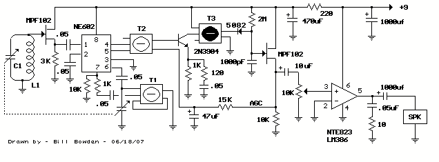
Pictured above is a little AM superhetrodyne receiver that covers the broadcast band from 550 Khz to 1650 Khz. The circuit employs the 8 pin Signetics balanced mixer IC (NE602) which converts the incoming RF signal to the standard...
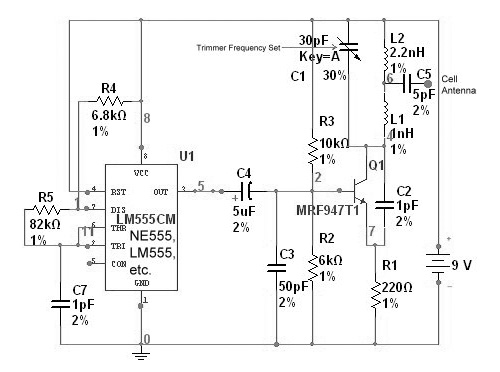
The circuit is based on the NE555 timer, functioning as a simple noise maker, with its output connected to a single transistor oscillator. This oscillator is designed to operate within a frequency range of 800 MHz to 2 GHz,...
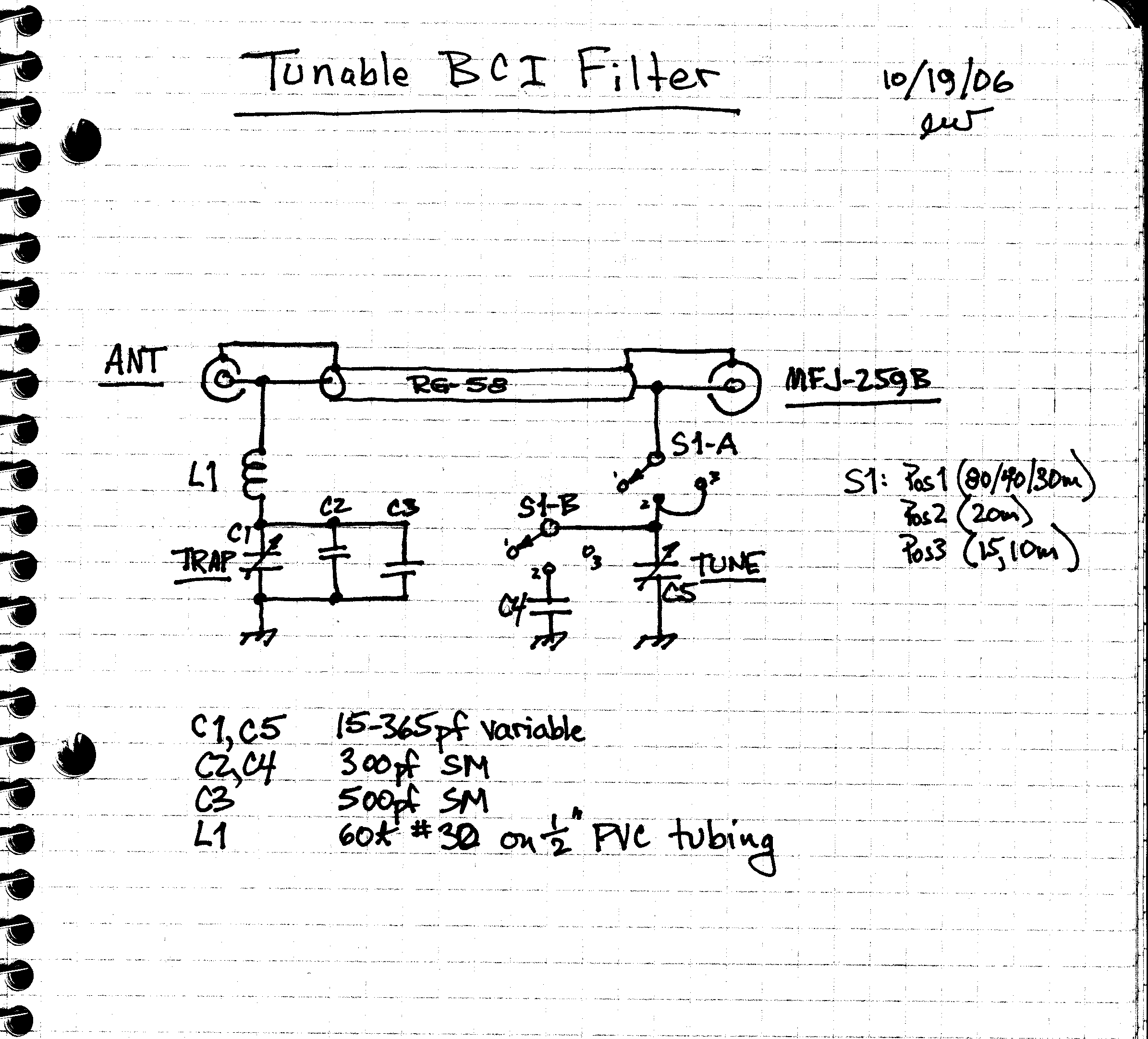
The design involves creating an AM broadcast signal eliminator. An undesired AM broadcast signal is directed to ground using a series resonant circuit composed of inductor L1 and capacitors C1, C2, and C3. At high frequencies, this series circuit...
The LED arrangement in the LM339 circuit consists of two rows of three LEDs, with each LED connected in parallel. The two rows are connected in parallel but with reversed polarity. The sensor array is composed of three west-facing...